Method for making an improved thin film solar cell interconnect using etch and deposition process

a technology of solar cell and interconnection, applied in the field of photovoltaic devices, can solve the problems of low throughput of laser ablation for panels with a large number of narrow strips, damage at the edge, and suffer from certain drawbacks, so as to improve the current transport in the structure

Inactive Publication Date: 2007-10-11
APPLIED MATERIALS INC
View PDF13 Cites 112 Cited by
  • Summary
  • Abstract
  • Description
  • Claims
  • Application Information

AI Technical Summary

Benefits of technology

[0014] The present invention provides a method of forming interconnects in a photovoltaic module. According to one aspect, a method according to the invention includes processing steps that are similar to those performed in conventional integrated circuit fabrication. For example, the method can include masks and etches to form isolation grooves between cells, and additional etches to form a conductive step adjacent to the grooves that can be used to form interconnects between cells. According to another aspect the method for forming the conductive step can be self-aligned, such as by positioning a mirror above the module and exposing photoresist from underneath the substrate at an angle one or more times, and etching to expose the conductive step. According to another aspect, the process can include steps to form grid lines in the module to improve current transport in the structure.

Problems solved by technology

While the method of the co-pending application provides acceptable results and much narrower interconnects than previously possible, it may suffer from certain drawbacks.
Moreover, laser ablation may have low throughput for panels with a large number of narrow stripes, where several hundred cuts, each one or meter long, may be required.
Still further, laser ablation can cause damage at the edge, especially when performed at high ablation rates.
Although these references depict an insulator within isolation grooves, the particular method used to accomplish this insulation is not disclosed, and thus cannot serve to improve the processes of the co-pending application.

Method used


Image

  • Method for making an improved thin film solar cell interconnect using etch and deposition process
  • Method for making an improved thin film solar cell interconnect using etch and deposition process
  • Method for making an improved thin film solar cell interconnect using etch and deposition process

Examples


Embodiment Construction

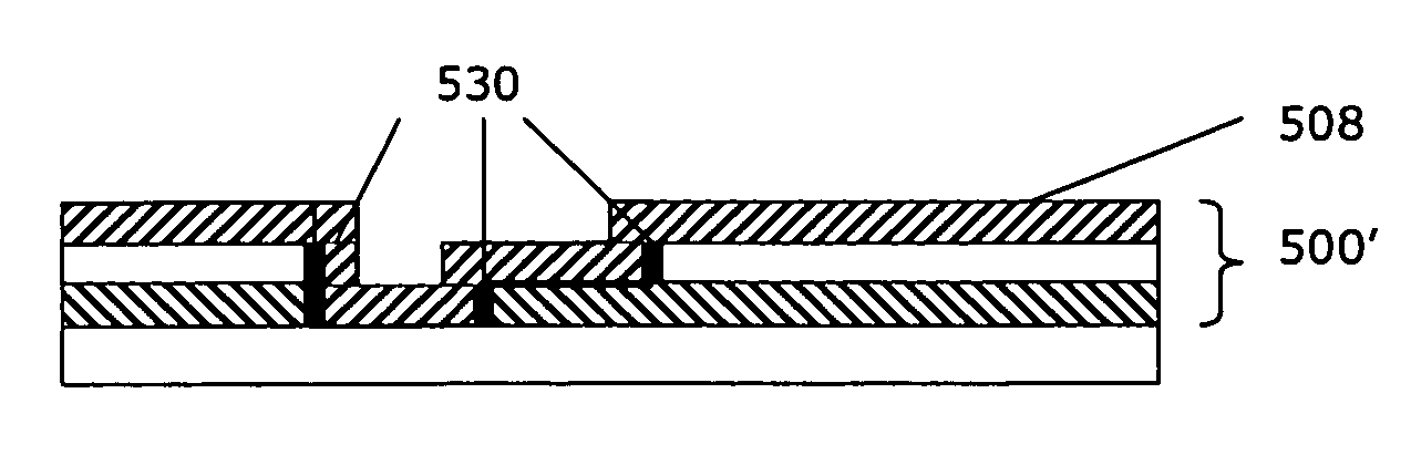
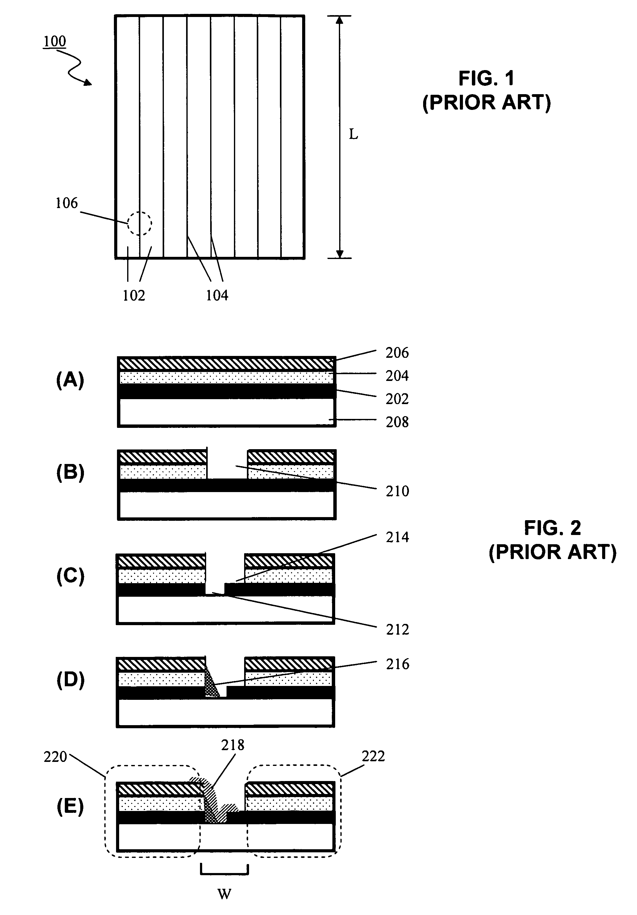
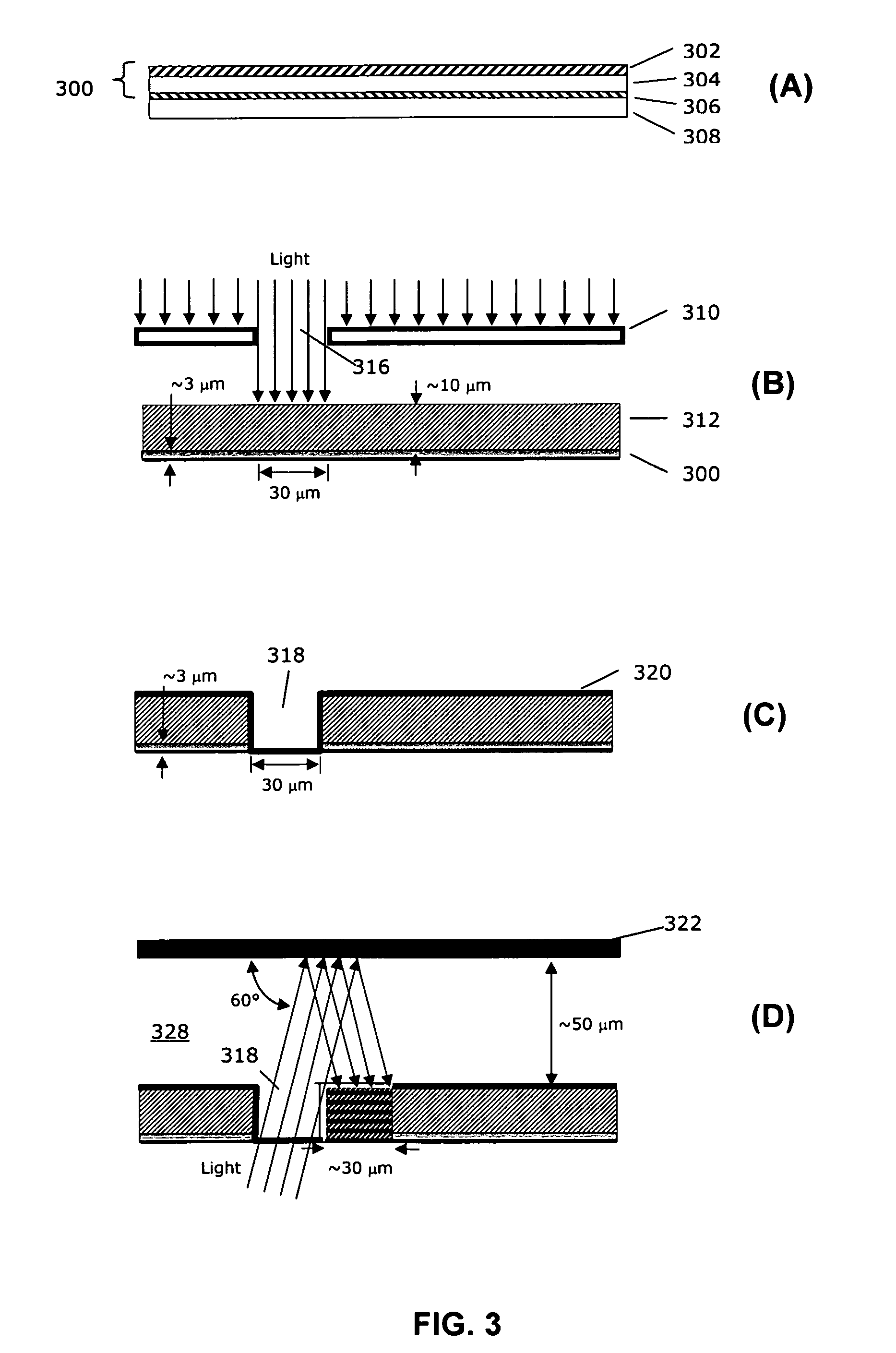
[0082] The present invention will now be described in detail with reference to the drawings, which are provided as illustrative examples of the invention so as to enable those skilled in the art to practice the invention. Notably, the figures and examples below are not meant to limit the scope of the present invention to a single embodiment, but other embodiments are possible by way of interchange of some or all of the described or illustrated elements. Moreover, where certain elements of the present invention can be partially or fully implemented using known components, only those portions of such known components that are necessary for an understanding of the present invention will be described, and detailed descriptions of other portions of such known components will be omitted so as not to obscure the invention. In the present specification, an embodiment showing a singular component should not be considered limiting; rather, the invention is intended to encompass other embodime...


PUM


Abstract

The present invention provides a method of forming interconnects in a photovoltaic module. According to one aspect, a method according to the invention includes processing steps that are similar to those performed in conventional integrated circuit fabrication. For example, the method can include masks and etches to form isolation grooves between cells, and additional etches to form a conductive step adjacent to the grooves that can be used to form interconnects between cells. According to another aspect the method for forming the conductive step can be self-aligned, such as by positioning a mirror above the module and exposing photoresist from underneath the substrate at an angle one or more times, and etching to expose the conductive step. According to another aspect, the process can include steps to form grid lines in the module to improve current transport in the structure.

Description

FIELD OF THE INVENTION [0001] The present invention relates generally to photovoltaic devices, and more particularly to a system and method for making improved interconnects in thin-film photovoltaic devices. BACKGROUND OF THE INVENTION [0002] Thin film solar modules offer an attractive way to achieve low manufacturing cost with reasonable efficiency. These modules are made from a variety of materials, including amorphous silicon, amorphous silicon germanium, copper indium gallium selenide (CIGS), and cadmium telluride. A common feature of these solar modules is the deposition on a large area insulator such as a glass sheet. [0003] Another common feature of these modules is the use of scribes and interconnects to divide the large area deposited layer into a number of cells and / or sub-cells. A top view of a typical module divided in this fashion is shown in FIG. 1. As shown in FIG. 1, a module 100 is divided into a plurality of cells 102 (i.e. stripes) that are series connected (e.g....

Claims


Application Information

Patent Timeline
Patent Type & Authority Applications(United States)
IPC IPC(8): H01L21/4763
CPCY02E10/50H01L31/0463
Inventor BORDEN, PETER
Owner APPLIED MATERIALS INC
Why Eureka
Try Eureka