Liquid crystal display device

a technology of liquid crystal display and display panel, which is applied in the direction of static indicating devices, non-linear optics, instruments, etc., can solve the problems of poor improvement of the contrast ratio obtained by luminance control of backlight, insufficient live performance, and lower contrast ratio of lcd panel alone in a dark environment, so as to suppress the degradation of image quality

Active Publication Date: 2007-10-18
NEC LCD TECH CORP
View PDF4 Cites 64 Cited by
  • Summary
  • Abstract
  • Description
  • Claims
  • Application Information

AI Technical Summary

Benefits of technology

[0013]In view of the above problem of the conventional multi-panel LCD device, it is an object of the present invention to provide a multi-panel LCD...

Problems solved by technology

However, there is a defect in the LCD device that the contrast ratio of the LCD panel alone in a dark environment is lower than that of a CRT, that (3000:1) of a plasma display panel, which are also used as a television monitor similarly to the LCD panel, and that of a field-emission display panel called FED/SED, and is at most on the order of 1000:1.
Therefore, there is pointed out the problem of insufficient feeling of live performance during representing image sources such as a motion picture having a higher power of expression especially in the dark area.
Thus, if there are a high luminance area and a low luminance area concurrently represented on the same screen of the LCD device, the luminance of the backlight cannot be regulated area by area, resulting in a poor improvement of the contrast ratio obtained by the luminance control of the backlight.
However, such a com...

Method used


Image

  • Liquid crystal display device
  • Liquid crystal display device
  • Liquid crystal display device

Examples


first embodiment

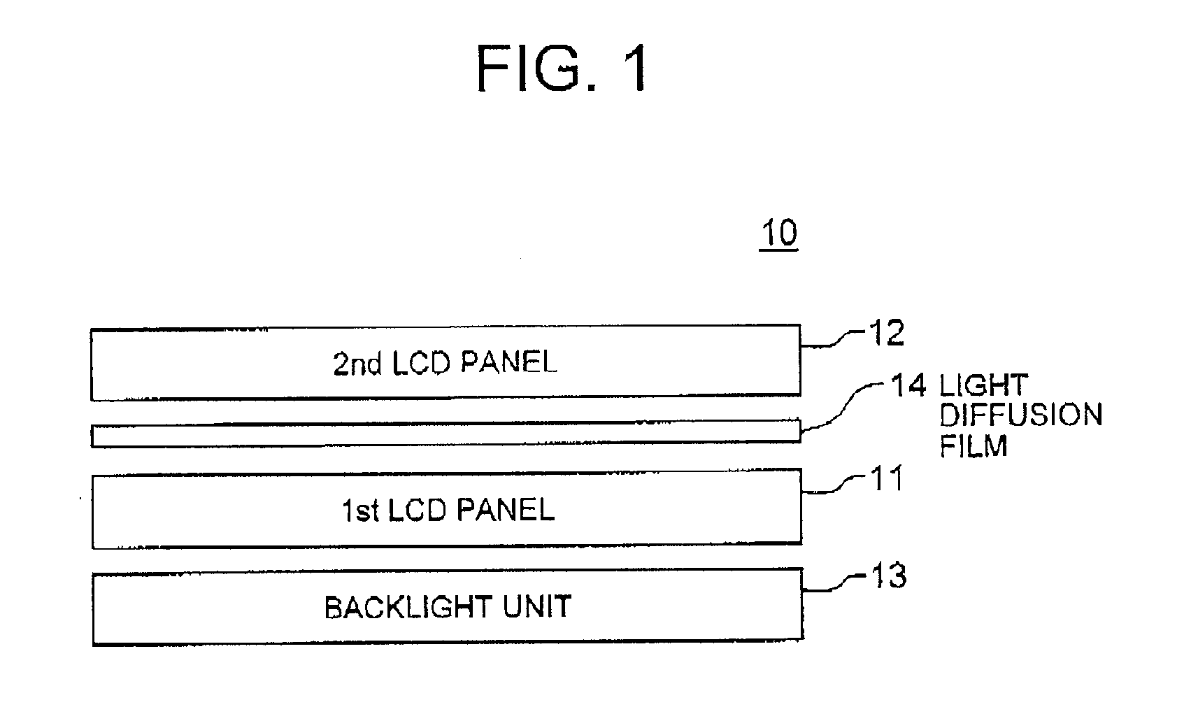
[0046]Now, embodiments of the present invention will be described in detail with reference to the accompanying drawings. FIG. 1 is a sectional view showing the configuration of a LCD device according to the present invention. The LCD device, generally designated by numeral 10, includes a first LCD panel 11 as a rear-side LCD panel, a second LCD panel 12 as a front-side LCD panel, a backlight unit 13 disposed at the rear of the first LCD panel 11, and a light diffusion layer 14 interposed between the first LCD panel 11 and the second LCD panel 12.

[0047]The first and second LCD panels 11 and 12 each include a pair of transparent substrates opposed to each other with a predetermined distance therebetween, a liquid crystal layer sandwiched between the transparent substrates, and a pair of polarizing films each arranged on the surface of a corresponding one of the transparent substrates far from the liquid crystal (LC) layer. Further, at least one of the first and second LCD panels 11 an...

second embodiment

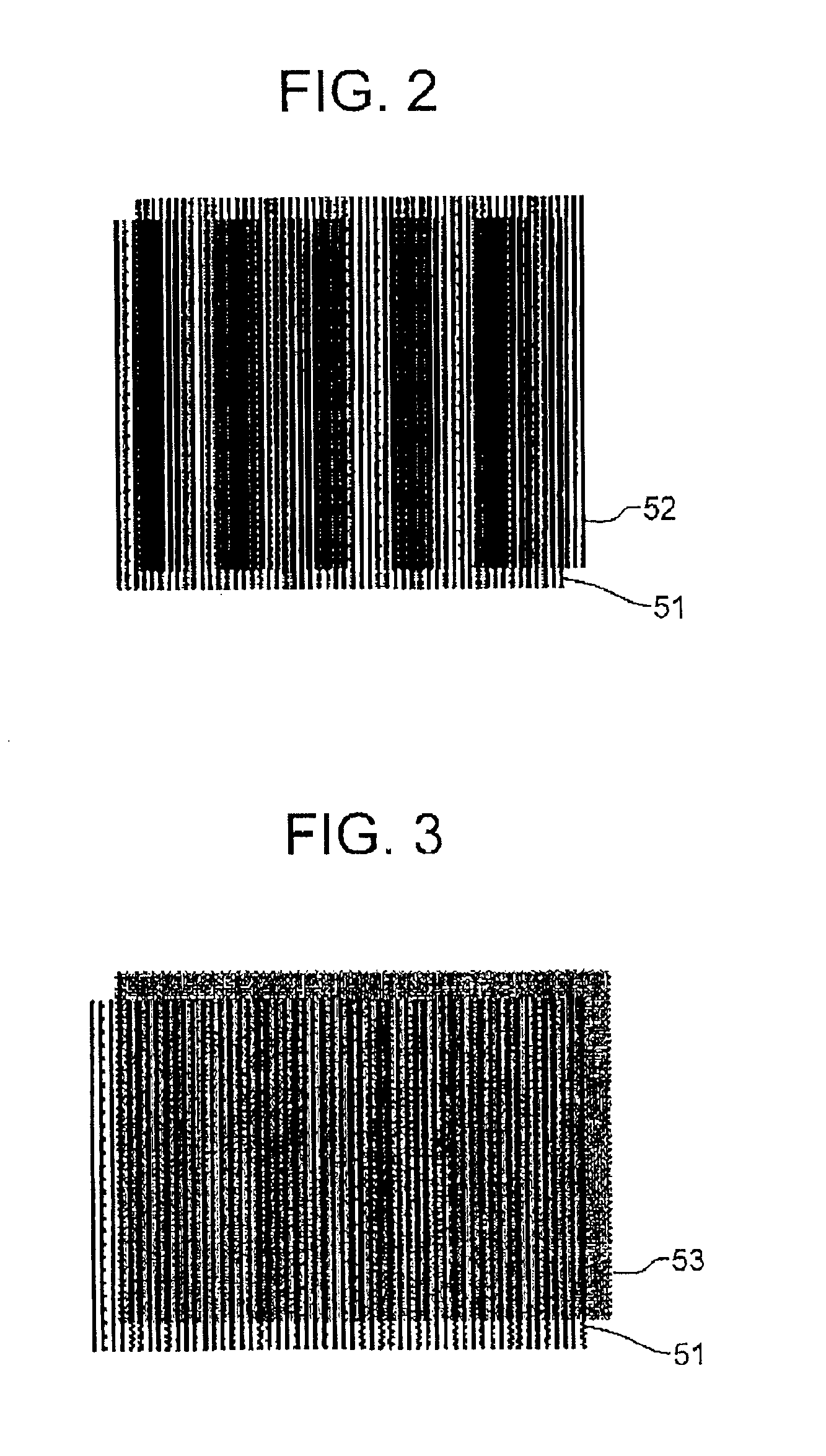
[0095]FIG. 17 is a top plan view of a typical pixel in the LCD panels 11 and 12 in the The pixel shown in FIG. 3 belongs to the first LCD panel 11, for example. The pixel is associated with a signal line or gate line 21 extending along a row direction 301, a data line 22 extending along a direction 302, and a TFT (thin-film transistor) 24 disposed in the vicinity of an intersection between the signal line 21 and the data line 22. On / off of the TFT 124 is controlled by the potential of the signal line 21.

[0096]The pixel includes a pixel electrode having comb-shape teeth 25 and connected to the data line 22 via the TFT 24, and a common electrode having comb-shape teeth 26 and surface electrode portion 27 which are connected to an inter-pixel common electrode line 23. Within the pixel area, the comb-shape teeth 25 of the pixel electrode oppose the comb-shape teeth 26 and surface electrode portion 27 of the common electrode to drive the LC layer by means of an electric field generated ...

fourth embodiment

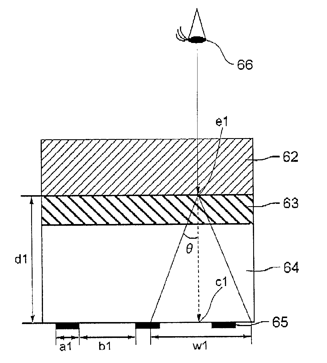
[0115]FIG. 22 shows a multiple-panel LCD device according to the present invention. The LCD device, generally designated by reference mark 10d, includes a backlight unit 13, a first LCD panel 11, a light condensing film 15, a light diffusion film 14 and a second LCD panel 12. The light condensing film 15 condenses the light emitted by the backlight unit 13 and passed by the first LCD panel, to pass the light toward the light diffusing film 14. The light diffusion film 14 diffuses the condensed light to the second LCD panel, thereby gradating the difference between the bright luminance and the dark luminance generated by the black matrix, while maintaining the condensed state of the light having a higher transmittance.

[0116]Examples of the material for the light condensing film 15 include an optical film such as described in Patent Publication JP-1999-508622. The optical film described therein mounts thereon a structure including a plurality of linear prisms. The linear prisms have a...


PUM


Abstract

A LCD device includes first and second LCD panels stacked one on another. Each of the first and second LCD panels includes a pair of transparent substrates, a liquid crystal layer sandwiched therebetween, and a pair of polarizing films sandwiching therebetween the pair of transparent substrates. A light diffusion layer having light diffusion function is interposed between the first LCD panel and the second LCD panel. The light diffusion layer reduces the intensity of the light passed by the first LCD panel, thereby alleviating the periodicity of the arrangement of dark areas and bright areas to alleviate the moire caused by light interference.

Description

[0001]This application is based upon and claims the benefit of priority from Japanese patent application No. 2006-114085 filed on Apr. 18, 2006, and Japanese patent application No. 2007-108283 filed on Apr. 17, 2007, the disclosure of which is incorporated herein in its entirety by reference.BACKGROUND OF THE INVENTION[0002]1. Field of the Invention[0003]The present invention relates to a liquid crystal display (LCD) device, and more particularly to a direct-view-type LCD device capable of achieving a higher contrast ratio.[0004]2. Description of the Related Art[0005]LCD devices have the advantage of realizing a higher definition with a lower power dissipation and are used for a wide range of applications from a small-screen cellular phone to a large-screen television monitor. However, there is a defect in the LCD device that the contrast ratio of the LCD panel alone in a dark environment is lower than that of a CRT, that (3000:1) of a plasma display panel, which are also used as a ...

Claims


Application Information

Patent Timeline
IPC IPC(8): G09G3/36
CPCG02F1/133504G02F2001/133565G02F1/1347G02F1/133526G02F1/133565G02F1/1335
Inventor KITAGAWA, YOSHIROIKENO, HIDENORIUEHARA, SHINICHIYATSUSHIRO, TAKASHI
Owner NEC LCD TECH CORP
Why Eureka
Try Eureka