Electrophotographic photosensitive member

a photosensitive member and electrophobic technology, applied in the field of electrophobic photosensitive members, can solve the problems of reducing sensitivity, degrading image quality, and unnecessarily requiring such heaters, and achieves excellent charging ability, sensitivity and electric potential properties, and energy saving.

Inactive Publication Date: 2009-03-03
CANON KK
View PDF26 Cites 26 Cited by
  • Summary
  • Abstract
  • Description
  • Claims
  • Application Information

AI Technical Summary

Benefits of technology

[0017]The present invention has been achieved for the purpose of improving the above described problems. An object of the present invention is to provide an electrophotographic photosensitive member having excellent electric potential properties and being capable of suppressing the image quality degradation caused by interference when used in an electrophotographic apparatus which meets energy saving and image quality improvement.
[0019]As will be described below, in the present invention, by using a metal fluoride in the surface layer of the electrophotographic photosensitive member, and moreover, by providing at least one intermediate layer composed of a metal oxide between the photoconductive layer and the surface layer, there can be obtained an electrophotographic photosensitive member which is excellent in charging ability, sensitivity and electric potential properties such as residual electric potential even in an electrophotographic apparatus which does not use a heater for heating the electrophotographic photosensitive member so as to meet energy saving.

Problems solved by technology

However, when an a-SiC:H film is used as the surface layer, low-resistant substances such as moisture are adsorbed on the film in a high-humidity environment to tend to decrease the surface resistance and the charge retention ability, and consequently the electrostatic latent image pattern collapses to cause image defects such as image blurring and image deletion, so that sometimes a countermeasure against such resistance decrease of the surface layer is adopted in which the electrophotographic photosensitive member is heated.
However, from the viewpoint of energy saving, it is demanded to unnecessitate such a heater.
However, an a-C:H film tends to absorb image exposure light, resulting in decrease of the sensitivity thereof.
Additionally, while the electrophotographic photosensitive member is used repeatedly, an nonuniform abrasion thickness of the a-C:H film, if any, causes the sensitivity nonuniformity, which sometimes leads to the image density nonuniformity to degrade the image quality.
However, the spot diameter cannot be reduced beyond the diffraction limit determined by the wavelength of the exposure laser light and the aperture ratio of the imaging lens, and the requirements for the size increase of the lens and the mechanical precision improvement inevitably involve the increases of the apparatus size and the cost.
For example, when the resolution is enhanced by reducing the spot diameter of the exposure laser light, there is a fear that even-such image deletion as nonconspicuous with a conventional spot diameter around 60 to 100 μm is sometimes manifested with an improved image resolution.
In addition, although metal fluorides such as magnesium fluoride hardly generate image deletion ascribable to the high-humidity environment, image defect accompanying image deletion sometimes tends to occur.
Moreover, when a magnesium fluoride film is used for the surface layer, the interference is manifested between the exposure laser light component which is reflected on the interface between the surface layer and the photoconductive layer and reaches the uppermost surface of the surface layer and the exposure laser light component which is reflected on the uppermost surface of the surface layer, and consequently sometimes the image quality is degraded.
Consequently, interference tends to degrade the image quality when the exposure laser light tends to be reflected between the photoconductive layer and the surface layer because of the small roughness of the photoconductive layer surface and the like reasons.

Method used


Image

  • Electrophotographic photosensitive member
  • Electrophotographic photosensitive member
  • Electrophotographic photosensitive member

Examples


example 1

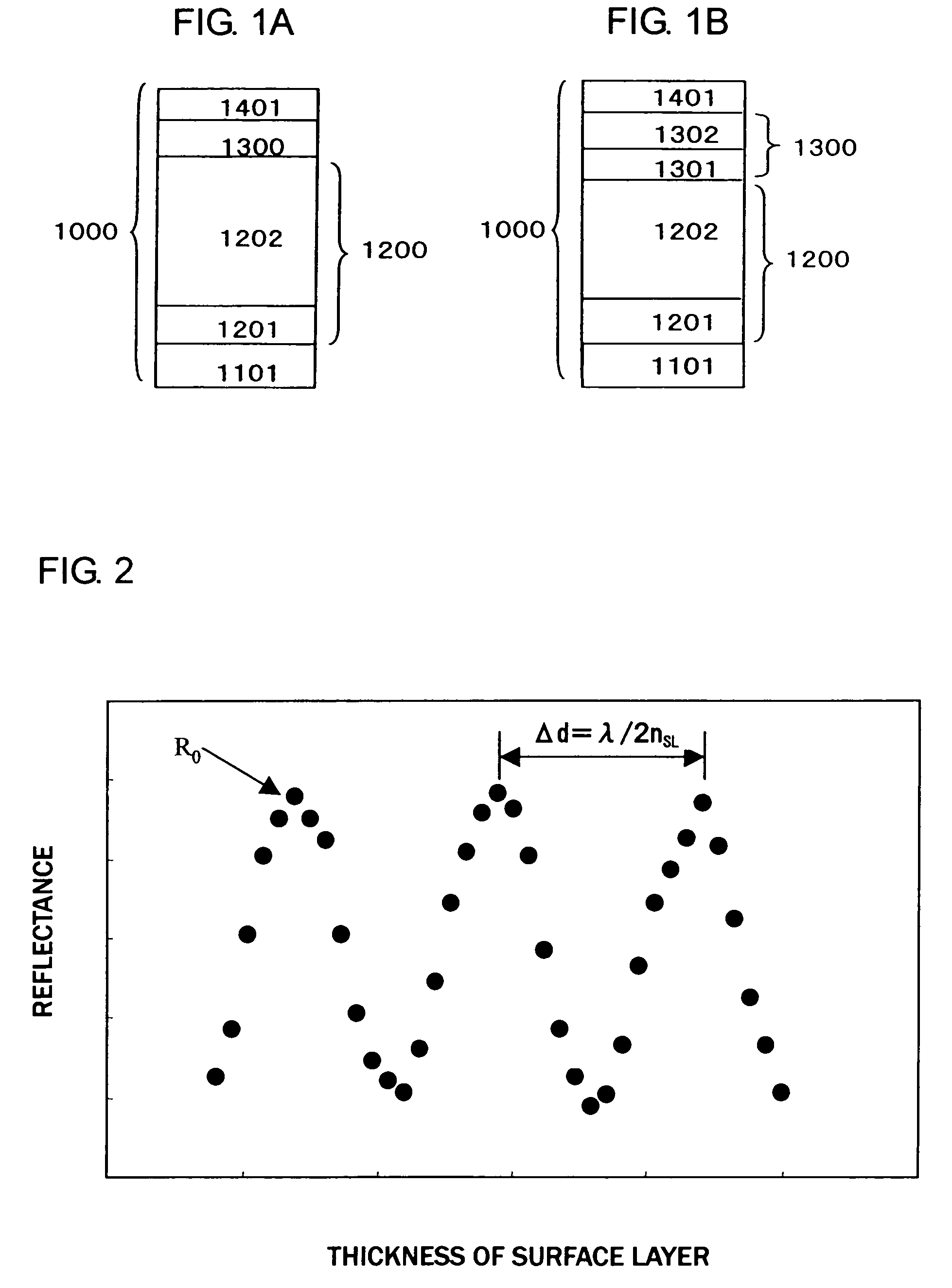
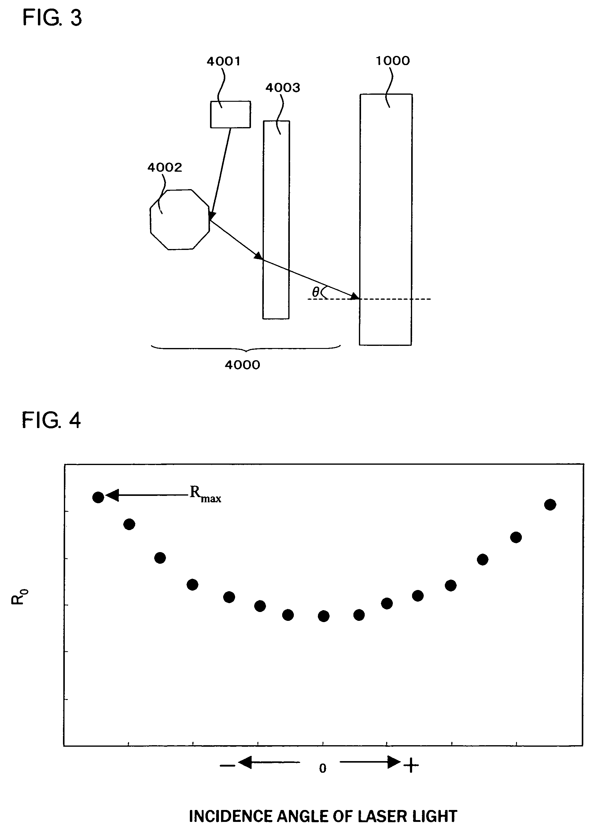
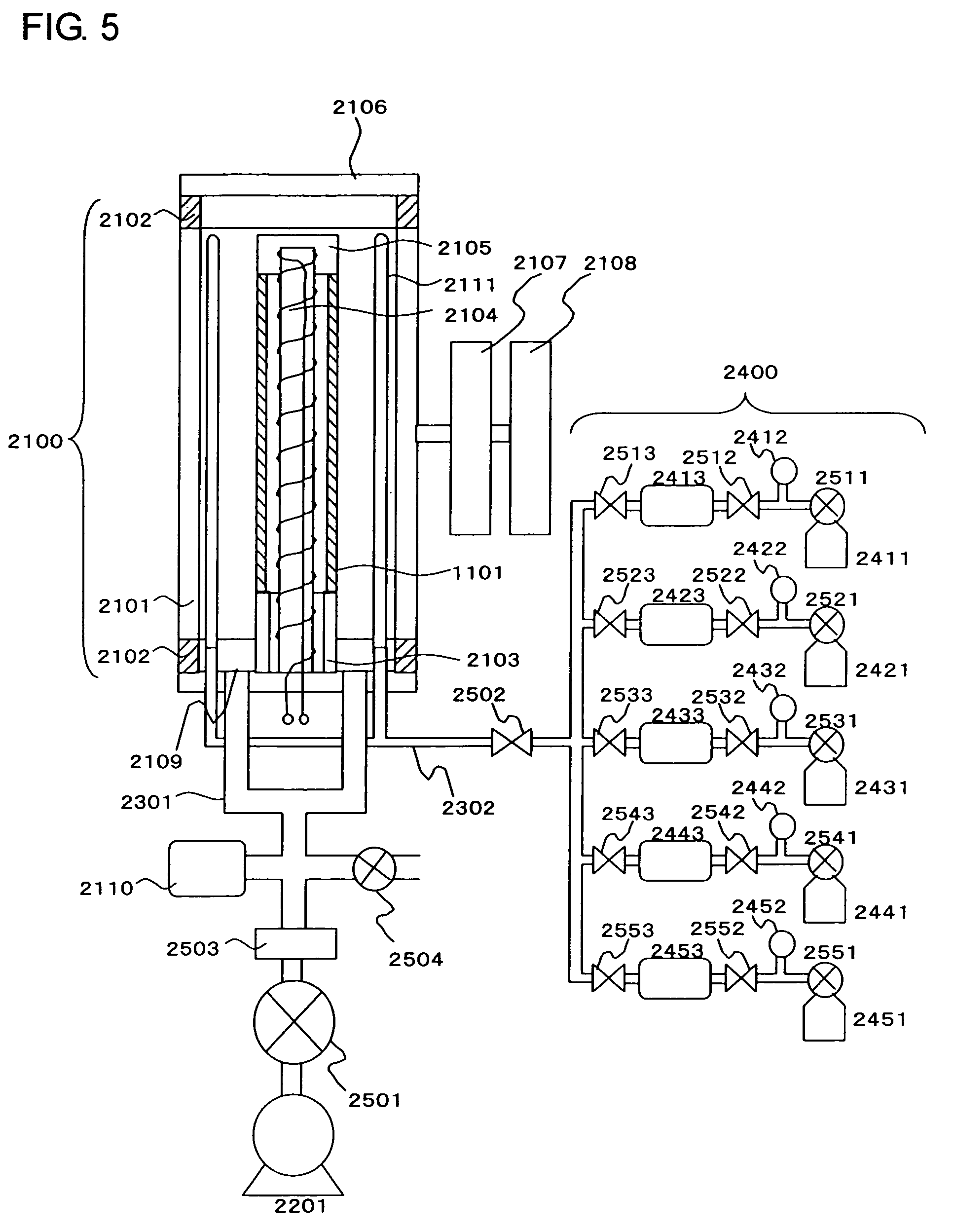
[0071]An amorphous silicon layer was formed by use of the CVD apparatus shown in FIG. 5, then an intermediate layer composed of a metal oxide and a surface layer composed of a metal fluoride are formed by use of the sputtering apparatus shown in FIG. 6 to produce an electrophotographic photosensitive member, and the electric potential properties thereof were evaluated.

[0072]First, a charge injection blocking layer and a photoconductive layer mainly composed of amorphous silicon were formed by use of the CVD apparatus shown in FIG. 5. As the substrate, an aluminum cylinder of 80 mm in diameter and 358 mm in length was used. The forming conditions of the amorphous silicon layer are shown in Table 1.

[0073]

TABLE 1Charge injectionPhotoconductiveblocking layerlayerGases and flow ratesSiH4 (ml / min. [normal])100100B2H6 (ppm, based on SiH4)20000.5NO (ml / min. [normal])5Substrate temperature (° C.)250250Pressure inside the7070reaction vessel (Pa)High frequency electric0.10.1power (kW)Thickness...

example 2

[0097]An amorphous silicon layer was formed by use of the CVD apparatus shown in FIG. 5, and then an intermediate layer composed of a metal oxide and a surface layer composed of a metal fluoride were formed by use of the sputtering apparatus shown in FIG. 6 to produce an electrophotographic photosensitive member for which the greatest value of reflectance was 20% or less. For the electrophotographic photosensitive member, the initial electric potential properties, the image in the print durability test, and the sensitivity nonuniformity, the sensitivity variation width and the greatest value of reflectance were evaluated.

[0098]In the present Example, an electrophotographic photosensitive member was produced by the same procedures as in Example 1, and the thickness values of the intermediate layer and the surface layer were made the same as those in Example 1. In the present Example, the constituents used respectively for the photoconductive layer, the intermediate layer and the surf...

examples 3 to 5

[0114]In each of Examples 3 to 5, an amorphous silicon layer was formed by use of the CVD apparatus shown in FIG. 5, then an intermediate layer composed of magnesium oxide and having a thickness different from that in Example 2 was formed by use of the sputtering apparatus shown in FIG. 6, and then a surface layer composed of magnesium fluoride was formed to produce an electrophotographic photosensitive member. For each of the produced electrophotographic photosensitive members, the initial electric potential properties, the image in the print durability test, the sensitivity nonuniformity, the sensitivity variation width and the greatest value of reflectance were evaluated.

[0115]In each of Examples 3 to 5, the same substrate as in Example 1 was used, and the formation procedures and the forming conditions for the charge injection blocking layer and the photoconductive layer were the same as in Example 1.

[0116]In each of Examples 3 to 5, after the charge injection blocking layer and...


PUM


Abstract

There is provided an electrophotographic photosensitive member used in an electrophotographic apparatus which meets energy saving and higher image quality. The electrophotographic photosensitive member has excellent potential properties, and can suppress the image quality degradation caused by interference. The electrophotographic photosensitive member of the present invention including on a conductive substrate at least a photoconductive layer mainly composed of amorphous silicon, a surface layer, and at least one intermediate layer interposed between the photoconductive layer and the surface layer, wherein the surface layer contains a metal fluoride (exclusive of silicon fluoride) and the intermediate layer contains a metal oxide.

Description

[0001]This application is a continuation of International Application No. PCT / JP2005 / 005072, filed on Mar. 15, 2005, which claims the benefit of Japanese Patent Application Nos. 2004-074414 filed on Mar. 16, 2004, and 2005-051085 filed on Feb. 25, 2005.BACKGROUND OF THE INVENTION[0002]1. Field of the Invention[0003]The present invention relates to an electrophotographic photosensitive member in which image exposure is conducted by use of laser light, in particular, an electrophotographic photosensitive member having excellent electric potential properties and excellent image quality when used in an electrophotographic apparatus which meets energy saving and a higher image resolution, and can also suppress nonuniformity and variation in sensitivity due to interference and further image defect caused by visualization of interference pattern.[0004]2. Related Background Art[0005]As a material for high-performance, high-durability and pollution-free electrophotographic photosensitive mem...

Claims


Application Information

Patent Timeline
Patent Type & Authority Patents(United States)
IPC IPC(8): G03G5/14G03G5/08G03G5/082G03G15/04G03G15/043
CPCG03G5/08214G03G5/08221G03G5/08235G03G5/0825G03G5/08278G03G5/144
Inventor TANIGUCHI, TAKAHISAAKIYAMA, KAZUYOSHI
Owner CANON KK
Why Eureka
Try Eureka