Electrostatic Chuck

a technology of electrostatic chuck and chuck body, which is applied in the direction of sleeves/socket joints, pipe joints, electrical appliances, etc., can solve the problems of reducing the yield of semiconductor elements in wafers, and achieve the effect of small temperature differences

Active Publication Date: 2007-10-25
KYOCERA CORP
View PDF12 Cites 27 Cited by
  • Summary
  • Abstract
  • Description
  • Claims
  • Application Information

AI Technical Summary

Benefits of technology

[0019] The objective of the present invention is to provide an electrostatic chuck which can achieve a small temperature difference on the surface of a wafer that is heated while being chucked onto the upper surface of the electrostatic chuck.
[0021] A plurality of dotted protrusions is formed inside the annular gas groove and inside the circular gas recess to support the back face of a wafer. In a heating process, the electrostatic chuck of the present invention makes it possible to shorten the time required for reaching a saturated temperature state, and consequently to maintain the in-plane temperature difference in the wafer in a very small level in a normal state.

Problems solved by technology

Upon manufacturing a recently-developed high density semiconductor element, for example, a semiconductor element having a width of a circuit line of 65 nm, the above-mentioned low temperature portions tend to generate a defective semiconductor element, resulting in a reduction in the yield of the semiconductor elements in the wafer.

Method used


Image

  • Electrostatic Chuck
  • Electrostatic Chuck
  • Electrostatic Chuck

Examples


example 1

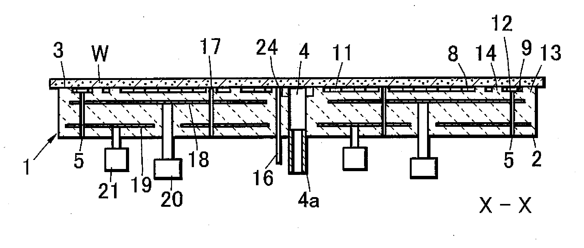
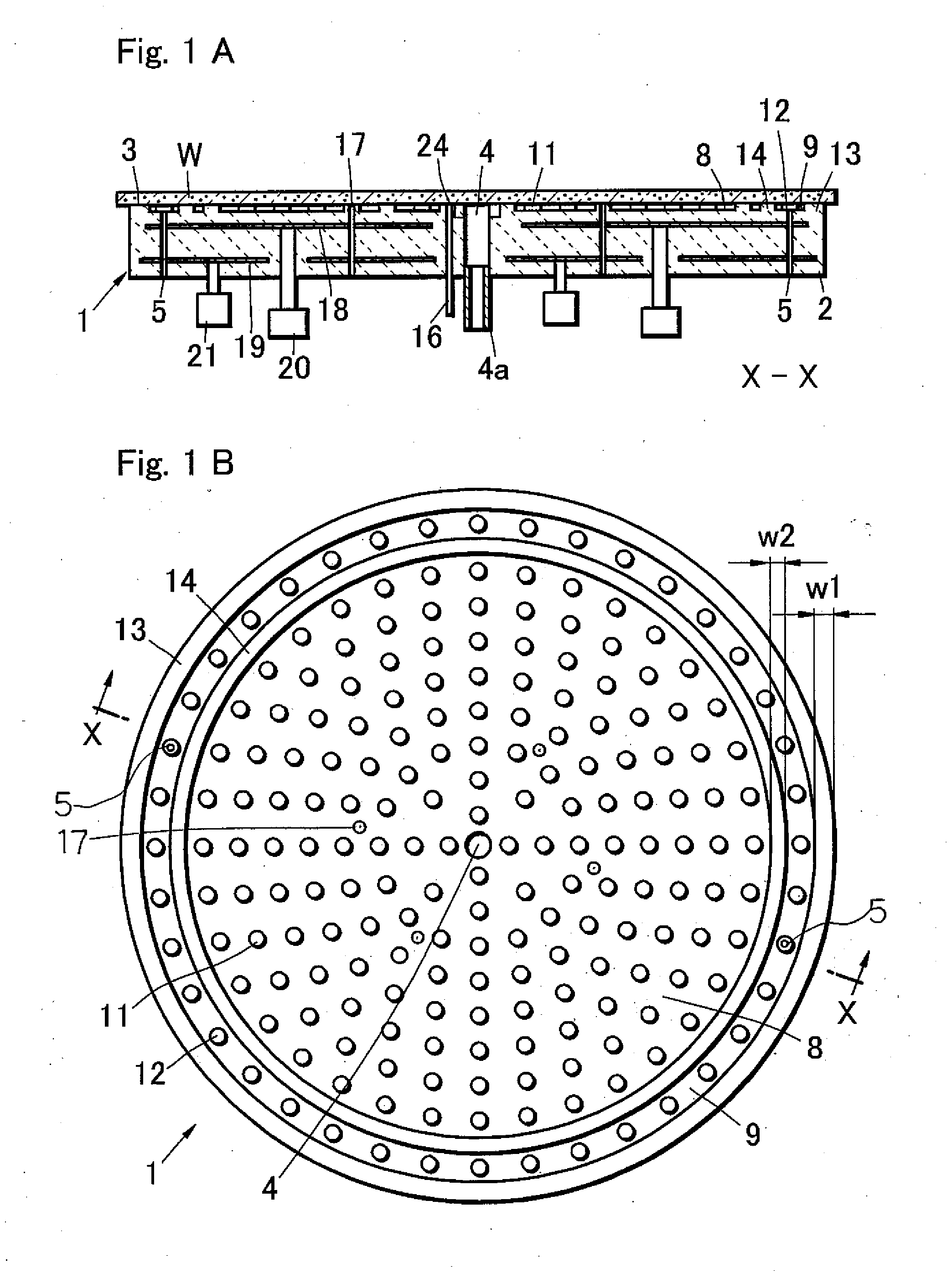
[0074] First, with respect to the circular gas recess 8 of the electrostatic chuck having an outer shape of the mounting surface 3 of 300 mm, the diameter thereof was varied to 60 to 97% of the outer shape of the mounting surface 3 to prepare respective electrostatic chucks that formed samples No. 6 to 12. Here, the ratio of the area of the protrusion inside the gas groove with respect to the circular gas recess 8 was set to 1. Moreover, the ratio of the area of the protrusion inside the gas groove with respect to the annular gas groove was also set to 1. Samples No. 1 to 5 were prepared for comparative examples. Table 1 shows the results of the tests.

TABLE 1sample12345789101112shape ofmountingsurfaceDc / D (%)—————607080909597wafer666552.52.0222.53temp. (° C.)time to1516141513976678saturatetemp. (s)

[0075] It was found that the electrostatic chucks of the present invention corresponding to samples No. 7 to 12 had in-plane temperature differences of the wafer within 3° C., which were...

example 2

[0078] Next, the same manufacturing processes as example 1 were carried out to prepare electrostatic chucks with the width W2 of the annular protrusion 14 surrounded by the outer circumference of the circular gas recess 8 and the inner circumference of the annular gas groove 9 and the width W1 of the annular protrusion 13 surrounded by the outer circumference of the mounting surface and the outer circumference of the annular gas groove being respectively set within a range from 0.2 to 7 mm; and the in-plane temperature difference of the wafer was measured.

[0079] No. 21 to 32 of Table 2 show the results.

TABLE 2sample212223242526272829303132shape ofmountingsurfacewidth (mm)0.211357333333of firstprotrusionwidth (mm)3433330.30.52357of secondprotrusionwafer321.51.523321.51.523temp. (° C.)time to965559854459saturatetemp. (s)

[0080] With respect to the samples Nos. 22 to 25 as well as 28 to 31, the widths of the annular protrusions 13 and 14 were respectively in ranges of 1 to 5 mm and 0...

example 3

[0085] Next, the same manufacturing processes as example 1 were carried out to prepare electrostatic chucks with the area S1 of the circular gas recess 8 and the total area S2 of the upper surfaces of the dotted protrusions 11 located inside the circular gas recess as well as the area S3 of the annular gas groove 9 and the area S4 of the upper surfaces of the protrusions 12 located inside thereof being respectively varied; thus, electrostatic chucks having varied ratios of S1 / S2 and S3 / S4 were manufactured, and the characteristics thereof were evaluated in the same manner as Example 1. The results of Sample Nos. 41 to 52 are shown in Table 3.

TABLE 3sample 414243444546474849505152shape ofmountingsurfaceS1 / S20.512456333333S3 / S43333330.512357wafer21.50.80.81.2221.40.70.81.52temp. (° C.)time to644346743346saturatetemp. (s)

[0086] With respect to samples Nos. 42 to 45 as well as 48 to 51, the value of S1 / S2 is in a range from 1 to 5, the value of S3 / S4 is in a range of 1 to 5, an in-pla...


PUM


Abstract

An electrostatic chuck is provided which includes a circular ceramic plate having an electrostatic attractive electrode, a mounting surface for supporting a wafer which is formed on one of the main surfaces of the circular ceramic plate, an annular gas groove formed on the periphery of the mounting surface in the form of concentric circles with a gas inlet communicating with the annular gas groove, and a circular gas recess formed inside the ceramic plate and surrounded by the annular gas groove with a gas inlet communicating with the circular gas recess, wherein the annular gas groove and the circular gas recess are independently separated from each other by an annular rib protrusion, with a plurality of dotted protrusions being formed within both the annular gas groove and the circular gas recess. This arrangement makes it possible to achieve a smaller in-plane temperature difference on the wafer placed on the mounting surface of the electrostatic chuck and a shorter saturating time into a predetermined constant temperature.

Description

BACKGROUND OF THE INVENTION [0001] 1. Field of the Invention [0002] The present invention relates to an electrostatic chuck which is used in an apparatus for manufacturing semiconductor devices or liquid crystal devices and mounts thereon a wafer such as a semiconductor wafer and a liquid crystal glass substrate. [0003] 2. Prior Art [0004] Conventionally, in manufacturing processes for semiconductor devices, in order to carry out processes such as film-forming processes and etching processes on wafers such as a silicon wafer with high precision, the wafer is required to be held while properly remaining in high degree of flatness. For such a holding means, electrostatic chucks have been proposed. [0005] The electrostatic chucks can easily fix a wafer thereon with a high degree of wafer flatness which is required for various processes such as film forming or etching processes. The chucks are also applicable even in a vacuum so that they have been widely incorporated in a wide variety ...

Claims


Application Information

Patent Timeline
Patent Type & Authority Applications(United States)
IPC IPC(8): H01L21/683H01L21/00H01L21/68
CPCH01L21/67109Y10T279/23H01L21/6831H01L21/68
Inventor NAKAMURA, TSUNEHIKO
Owner KYOCERA CORP
Why Eureka
Try Eureka