Piezoelectric device and method for producing same

a technology of piezoelectric devices and steps, applied in the direction of device material selection, generators/motors, impedence networks, etc., can solve the problems of increasing the number of steps, the piezoelectric device may collapse, and the cost is inevitable, so as to achieve the effect of not causing an increase in the cos

Active Publication Date: 2007-11-01
MURATA MFG CO LTD
View PDF6 Cites 238 Cited by
  • Summary
  • Abstract
  • Description
  • Claims
  • Application Information

AI Technical Summary

Benefits of technology

[0010] To overcome the foregoing problems, the present invention provides a piezoelectric device having resis

Problems solved by technology

However, in the case where after a piezoelectric device sealed with a buildup structure including a resin is mounted on a circuit substrate, the resulting component is resin-molded together with another chip such as a semiconductor chip, the piezoelectric device may collapse because resin molding is generally performed under high-temperature and high-pressure cond

Method used


Image

  • Piezoelectric device and method for producing same
  • Piezoelectric device and method for producing same
  • Piezoelectric device and method for producing same

Examples


example 1

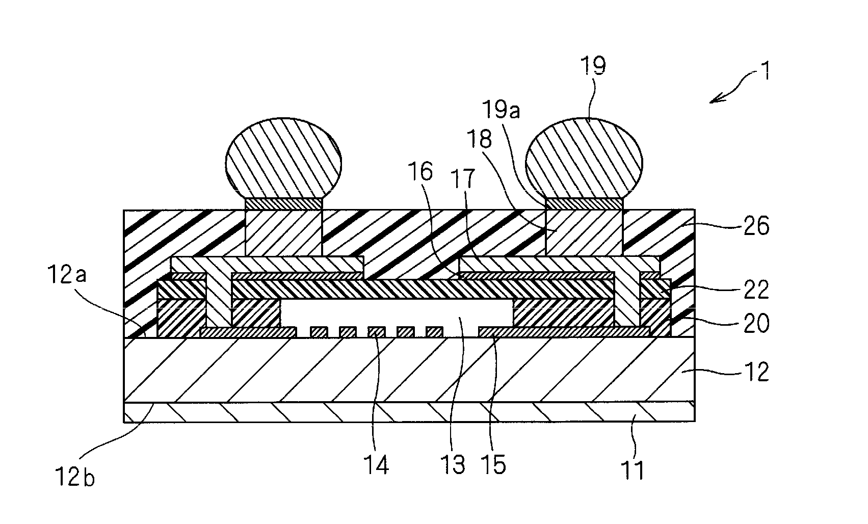
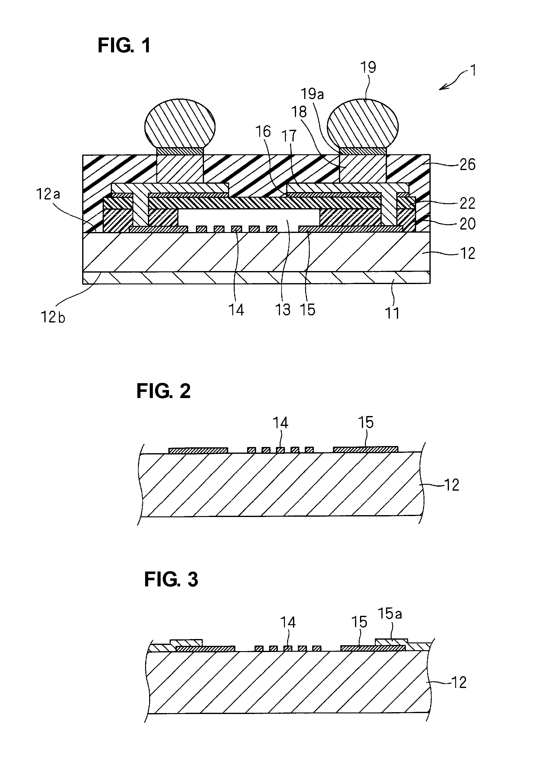
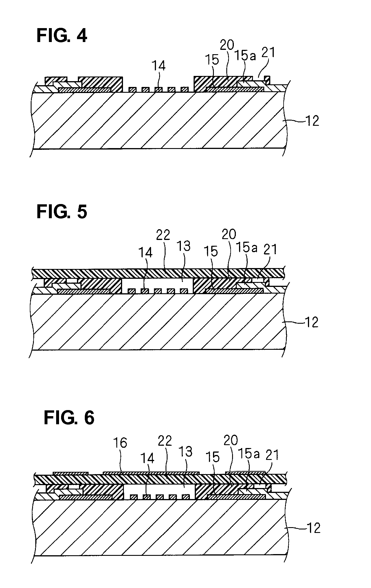
[0069] A piezoelectric device 10 according to EXAMPLE 1 will be described with reference to FIGS. 1 to 16.

[0070] Referring to FIG. 1 that is a cross-sectional view, the piezoelectric device 10 is a surface acoustic wave (SAW) filter. A conductive pattern including an interdigital transducer (IDT) 14 with interdigital electrodes, reflectors, pad electrodes 15, interconnection lines, and the like is formed on one main surface, i.e., a top surface 12a, of a piezoelectric substrate 12. A protective film 11 is formed on the other main surface, i.e., a bottom surface 12b, of the substrate 12. According to desired properties, a quartz substrate, a LiTaO3 substrate, LiNbO3 substrate, a substrate including a ZnO thin film, or other suitable material is used as the substrate 12.

[0071] A support layer 20, which is a first resin portion, is formed on the top surface 12a of the piezoelectric substrate 12 and on the pad electrodes 15 so as to surround the IDT 14. A cover layer 22, which is a se...

example 2

[0094] A piezoelectric device in EXAMPLE 2 will be described with reference to FIGS. 17 to 24. The piezoelectric device in EXAMPLE 2 preferably has substantially the same structure as that of the piezoelectric device 10 in EXAMPLE 1. Hereinafter, the same components as those of the piezoelectric device 10 in EXAMPLE 1 are designated using the same reference numerals, and differences from the piezoelectric device 10 in EXAMPLE 1 will be mainly described.

[0095]FIG. 17 corresponds to FIG. 7(a) described in EXAMPLE 1. Structures of metal films and plating films formed on a cover layer differ from those in EXAMPLE 1.

[0096] That is, the metal films and plating films have detour portions 17s and 17t deviating from an original wiring direction and expanded portions 17x and 17y each having a width larger than an original line width and cover a substantially overall surface above the sealed space 13. The detour portions 17s and 17t intersect repeatedly above the sealed space 13. The expande...

example 3

[0103] A piezoelectric device in EXAMPLE 3 will be described with reference to FIG. 25. The piezoelectric device in EXAMPLE 3has substantially the same structure as that of the piezoelectric device 10 in EXAMPLE 1. Hereinafter, the same components as those of the piezoelectric device 10 in EXAMPLE 1 are designated using the same reference numerals, and differences from the piezoelectric device 10 in EXAMPLE 1 will be mainly described.

[0104]FIG. 25 corresponds to FIG. 7 described in EXAMPLE 1. Unlike the structure in EXAMPLE 1, in the piezoelectric device in EXAMPLE 3, an additional layer 24 is formed on the cover layer 22. A metal film 16s is formed between the cover layer 22 and the additional layer 24. A plating film 17q is formed on a metal film 16t located on the additional layer 24.

[0105] The piezoelectric device in EXAMPLE 3 is produced in substantially the same way as the piezoelectric device 10 in EXAMPLE 1. The same steps are performed as those shown in FIGS. 2 to 6 accor...


PUM


Abstract

A piezoelectric device ensures resistance to molding without an increase in costs and includes an elemental substrate having a piezoelectric element and a conductive pattern electrically connected to the piezoelectric element; and insulating members disposed on the elemental substrate and surrounding the piezoelectric element leaving a space around the piezoelectric element. The insulating members have an internal conductor connected to the conductive pattern and extending apart from the elemental substrate. The internal conductor has expanded portions expanding in a direction intersecting the wiring direction of the internal conductor or a detour portion deviating from the wiring direction. The expanded portions or the detour portion crosses the boundary of a sealed space formed around the piezoelectric element.

Description

FIELD OF THE INVENTION [0001] The present invention relates to a piezoelectric device and a method for producing the same. In particular, the present invention relates to a piezoelectric device including a piezoelectric substrate and a piezoelectric element; and a method for producing the piezoelectric device. DESCRIPTION OF THE RELATED ART [0002] In piezoelectric devices, such as resonators and filters, including piezoelectric substrates and piezoelectric films, a construction in which piezoelectric vibration spaces are formed by mainly buildup structures including resins and the like has been known. [0003] For example, Japanese Unexamined Patent Application Publication No. 2004-165874 discloses that in a structure in which IDT electrodes overlaid with a cover and protruding electrodes protruding from pad electrodes, the protruding electrodes being disposed outside the cover, are disposed on a piezoelectric substrate and in which they are covered with an insulating layer and a resi...

Claims


Application Information

Patent Timeline
IPC IPC(8): H01L41/053H01L23/08H01L41/09H01L41/18H01L41/187H01L41/22H01L41/23H01L41/29H01L41/311H03H3/02H03H3/08H03H9/02H03H9/17H03H9/25H03H9/58
CPCH03H9/0576H03H9/059H03H9/725H03H9/72H03H9/1092H01L2224/11
Inventor IWAMOTO, TAKASHIKISHIMOTO, YASUNORI
Owner MURATA MFG CO LTD
Why Eureka
Try Eureka