Reference voltage generator circuit

a reference voltage and generator circuit technology, applied in the direction of electric variable regulation, process and machine control, instruments, etc., can solve the problem of error in the output reference voltage ascribable, the inability to independently measure the ptat voltage or the ctat voltage, and the inability to solve the base-emitter voltage vbe of the bipolar transistor. problem, to achieve the effect of accurate correction and low cos

Active Publication Date: 2007-11-01
SOCIONEXT INC
View PDF11 Cites 72 Cited by
  • Summary
  • Abstract
  • Description
  • Claims
  • Application Information

AI Technical Summary

Benefits of technology

[0050]It is an object of the present invention to provide a circuit for accurately correcting an output reference voltage of a reference voltage generation circuit at low cost.
[0054]Moreover, the first switch is on in a first operation mode and a third operation mode and is off in a second operation mode. The second switch is on in the first operation mode and the second operation mode and is off in the third operation Mode. Consequently, the current flowing to the first variable resistor is a current equal to the sum of a PTAT current and a CTAT current in the first operation mode, the CTAT current in the second operation mode, and the PTAT current in the third operation mode. Therefore, switching the operation modes makes it possible to measure a PTAT voltage or a CTAT voltage independently. This accordingly enables the PTAT voltage or the CTAT voltage to be corrected independently by adjusting values of the first and second variable resistors. As a result, the use of the circuit of the present invention can achieve accurate correction of an output reference voltage of the reference voltage generation circuit at low cost.

Problems solved by technology

But the output voltage of the bandgap circuit is influenced not only by the offset voltage of the operational amplifier but also by an error in resistors or in the base-emitter voltages Vbe of pnp bipolar transistors.
However, there is a problem that an error in the output reference voltage ascribable to variance in the resistors and the base-emitter voltages Vbe of the bipolar transistors is not solved.
However, with the conventional circuit configuration, it is not possible to independently measure the PTAT voltage or the CTAT voltage.
Therefore, accurate correction of the output reference voltage in a short test time (namely, at low cost) is difficult.
Therefore, the conventional resistor trimming circuit cannot be applied in typical and low-cost CMOS processes.

Method used


Image

  • Reference voltage generator circuit
  • Reference voltage generator circuit
  • Reference voltage generator circuit

Examples


first embodiment

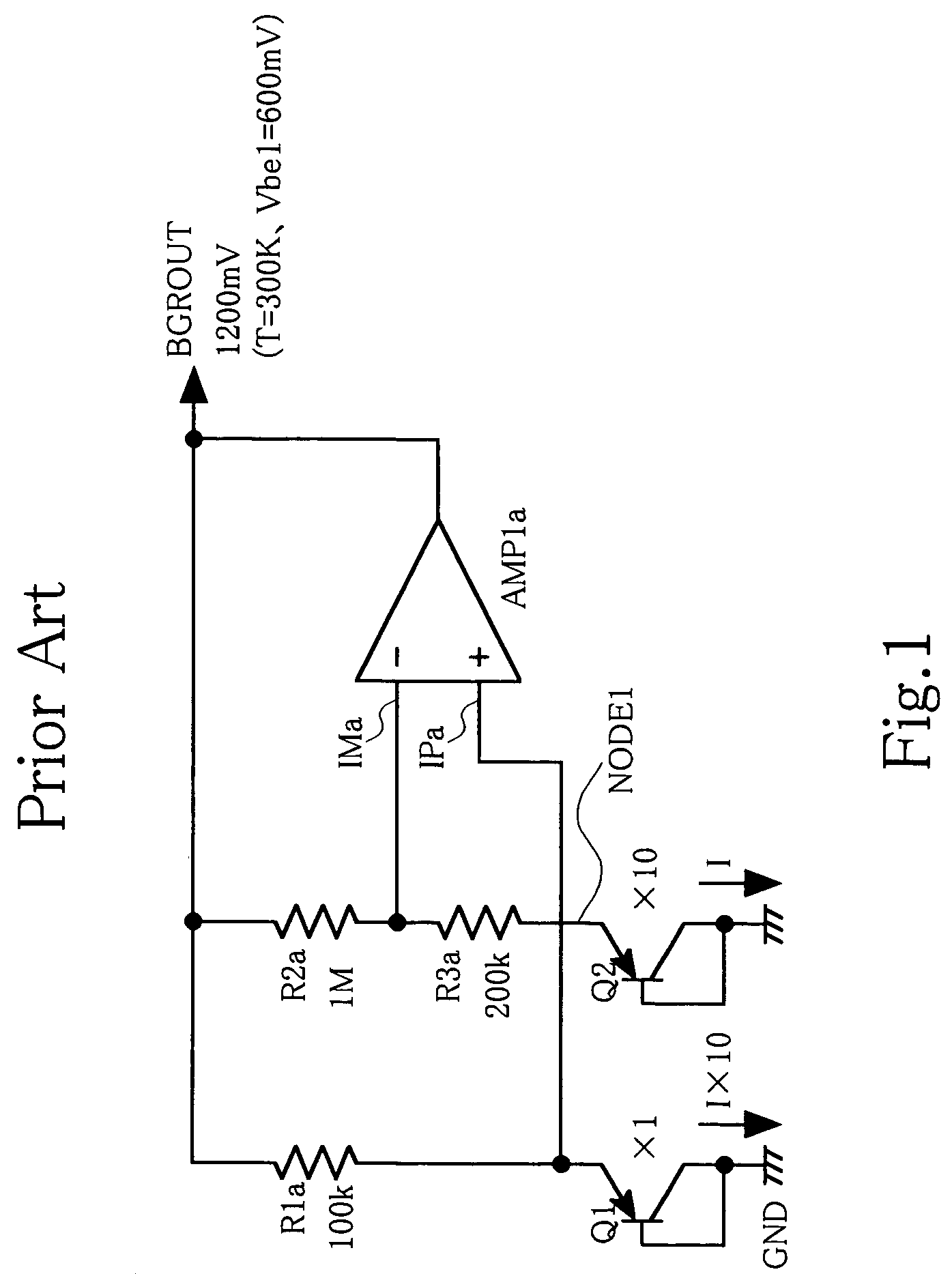
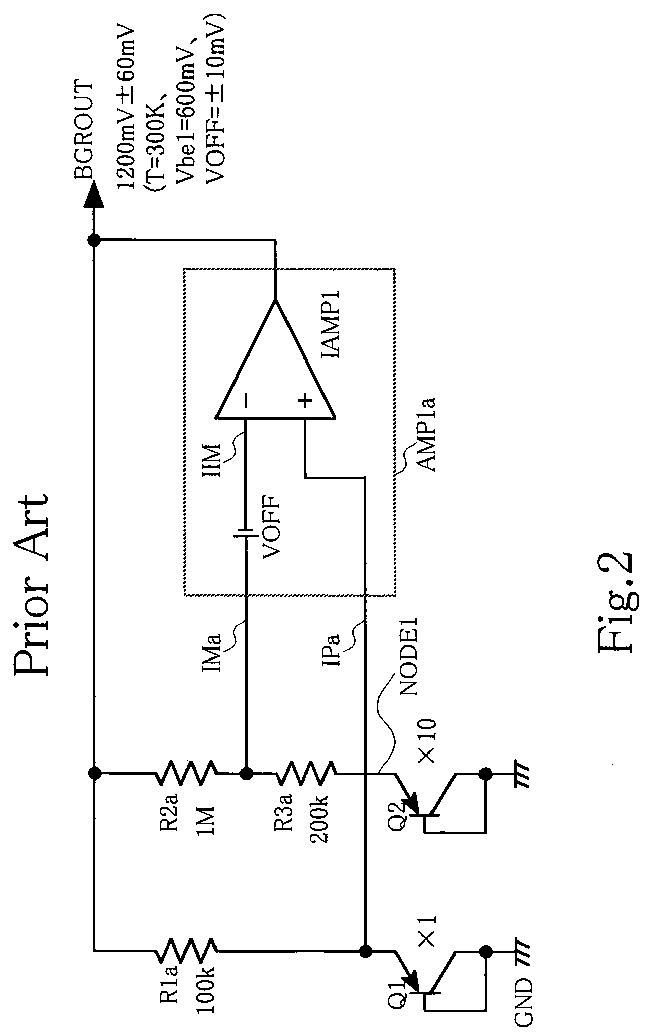
[0094]FIG. 9(a) and FIG. 9(b) show the present invention. A reference voltage generation circuit has pMOS transistors PM1-PM5, pnp bipolar transistors Q1, Q2 (hereinafter, also referred to simply as Q1, Q2), a resistor R1 (a resistance value thereof will be also denoted by R1), variable resistors VR1, VR2 (resistance values thereof will be also denoted by VR1, VR2), operational amplifiers AMP1, AMP2, and switches SW1 and SW2.

[0095]Sources of the transistors PM1-PM3 are connected to a VDD being a first power-supply line, gates thereof are connected to an output of the operational amplifier AMP1, and drains thereof are connected to a node IP being an emitter of the transistor Q1, the resistor R1, and the switch SW1 respectively. Sources of the transistors PM4 and PM5 are connected to the VDD, gates thereof are connected to an output of the operational amplifier AMP2, and drains thereof are connected to the variable resistor VR2 and the switch SW2 respectively. The operational amplifie...

second embodiment

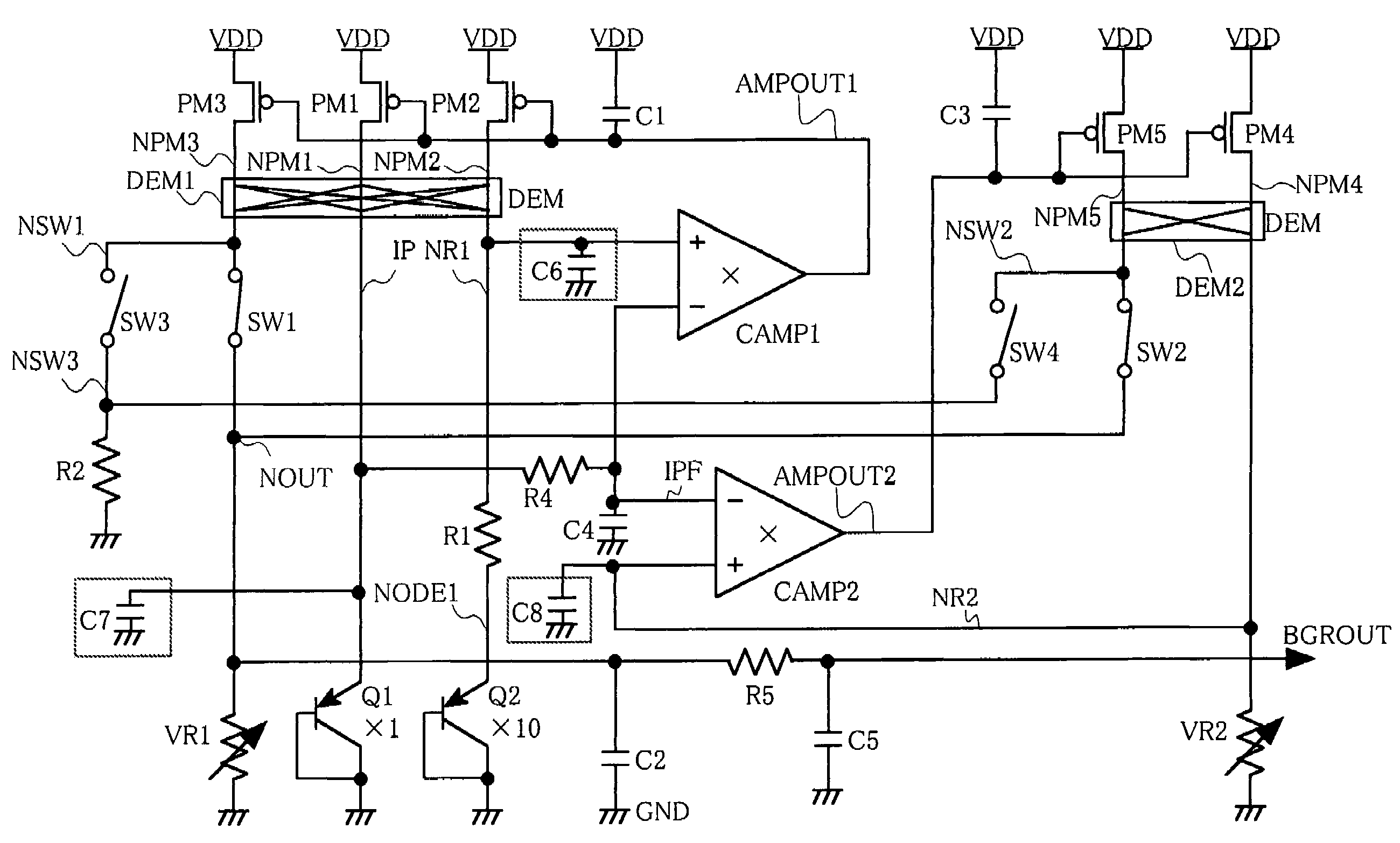
[0121]In the second embodiment described above, the influence of the offset voltage of the operational amplifier and the influence of mismatch of the MOS transistors working as current sources which are ascribable to manufacturing variance are reduced by using the dynamic element matching circuits DEM1, DEM2 and the chopper amplifiers CAMP1 and CAMP2. Consequently, the adjustment of the PTAT voltage and the CTAT voltage by the variable resistors VR1 and VR2 become more effective. That is, even by the adjustment at a given temperature, the PTAT voltage and the CTAT voltage can be accurately adjusted to design values in a wide temperature range. Further, by the switches SW3 and SW4, it is possible to control the PTAT current and the CTAT current flowing to the variable resistor VR1 so that the PTAT current and the CTAT current at the voltage adjustment time become equal to those at the actual usage time when the reference voltage is actually outputted. Consequently, it is possible to ...

third embodiment

[0125]The third embodiment described above has the buffer amplifier CAMP3. Consequently, even when the output impedance of the reference voltage BGROUT of the reference voltage generation circuit is high, it is possible to measure the PTAT voltage and the CTAT voltage stably. Therefore, it is possible to adjust the output reference voltage accurately at low cost.

[0126]FIG. 15 shows a fourth embodiment of the present invention. The same reference symbols are used to designate the same elements as the elements described in the second embodiment, and detailed description thereof will be omitted. A reference voltage generation circuit of this embodiment is structured such that a transistor PM6, a switch SW5, a resistor R3, and an AD converter ADC1 are added to the reference voltage generation circuit of the second embodiment. The transistor PM6, the switch SW5, and the resistor R3 are connected in series between a VDD and a GND. An input of the AD converter ADC1 is connected to a node T...


PUM


Abstract

A reference voltage generation circuit has transistors generating a PTAT current that increases in proportion to temperature, a transistor generating a CTAT current that decreases in proportion to temperature, a first variable resistor adjusting an output voltage, a transistor supplying the PTAT current to the first variable resistor via a first switch, a transistor supplying the CTAT current to the first variable resistor via a second switch, and a second variable resistor adjusting the CTAT current. The first switch is on in first and third operation modes and off in a second operation mode. The second switch is on in the first and second operation modes and off in the third operation mode. Switching the operation modes realizes independently outputting a PTAT voltage or a CTAT voltage. Independently adjusting the voltages makes it possible to correct output reference voltage of the reference voltage generation circuit accurately at low cost.

Description

CROSS REFERENCE TO RELATED APPLICATION[0001]This application is based upon and claims the benefit of priority from Japanese Patent Application No. 2006-127970, filed on May 1, 2006, the entire contents of which are incorporated herein by reference.BACKGROUND OF THE INVENTION[0002]1. Field of the Invention[0003]The present invention relates to a reference voltage generation circuit that outputs a reference voltage which does not depend on temperature.[0004]2. Description of the Related Art[0005]A reference voltage generation circuit called a bandgap circuit is generally in wide use for providing a reference voltage dependent neither on temperature nor on a power-supply voltage. For example, the bandgap circuit adds a voltage of a forward-biased pn junction and a PTAT (Proportional To Absolute Temperature) voltage that is proportional to absolute temperature (T). It is known that the voltage of the forward-biased pn junction, if approximated by a linear expression, exhibits negative l...

Claims


Application Information

Patent Timeline
Patent Type & Authority Applications(United States)
IPC IPC(8): G05F3/16
CPCG05F3/30
Inventor TACHIBANA, SUGURUARUGA, KENTAKATO, TATSUO
Owner SOCIONEXT INC
Why Eureka
Try Eureka