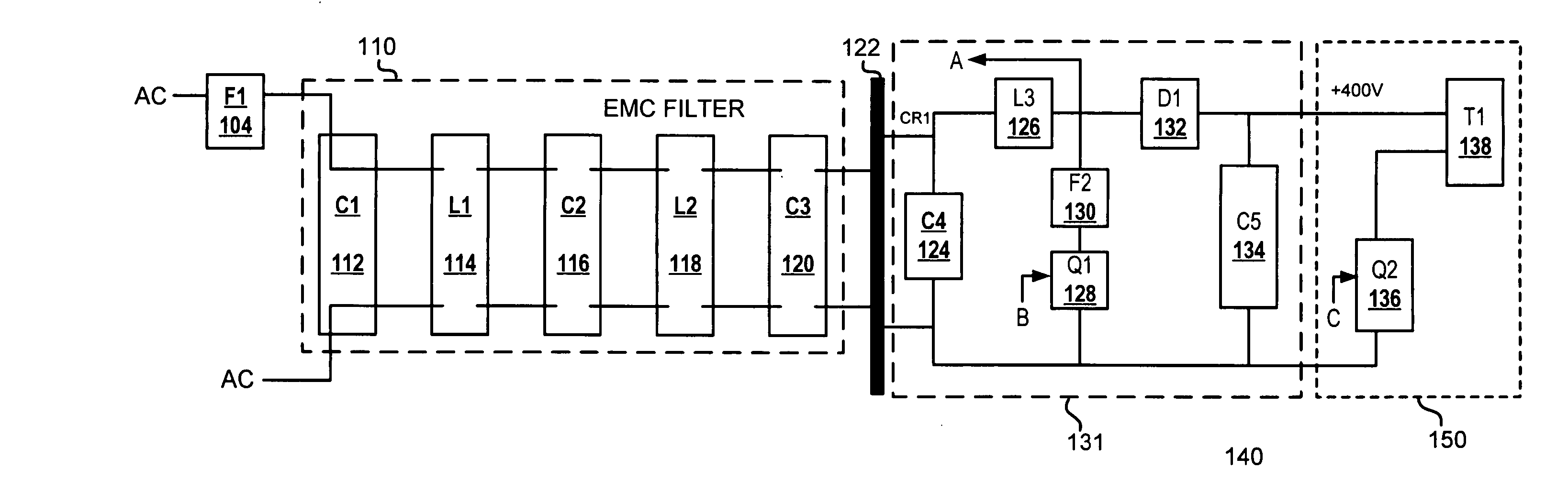
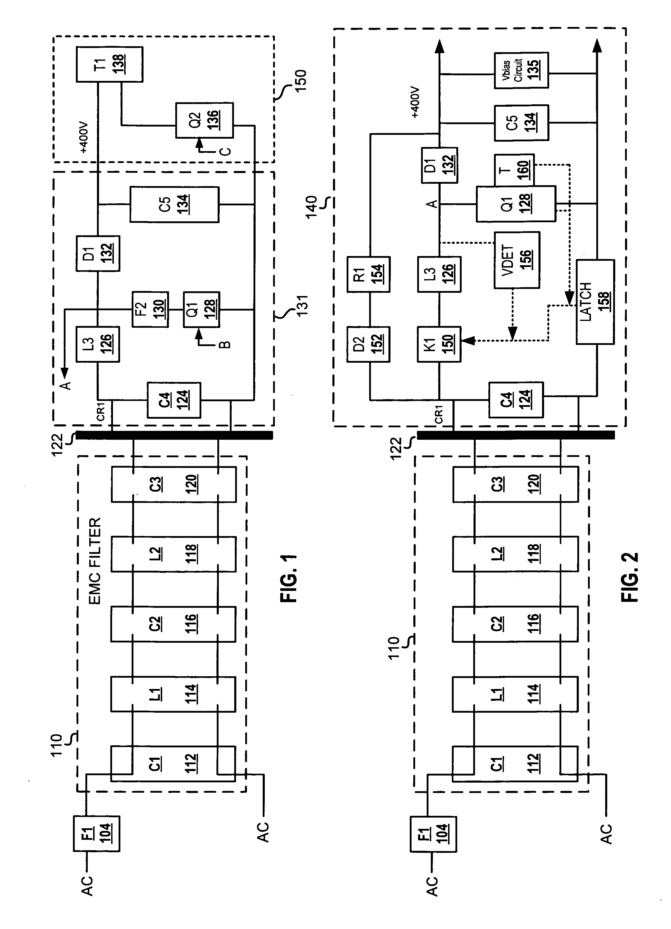
[0013] The present invention provides a circuit device and method for protecting electromagnetic compatibility (EMC) components from fault conditions that may negatively affect the components. In one implementation, a circuit device and method are provided to prevent high power dissipation in EMC components when/if the boost stage stops working or malfunctions. In another related implementation, an expanded circuit device and method prevents smoke and fire in case the boost stage switching device fails, shorts, or is defective.
[0014] The circuit device is designed so that the chopper stage (i.e., the stage that follows the boost stage) is latched off if/whenever the boost stage stops working. According to the methods of the invention, whenever such a fault occurs at the boost stage, the circuit immediately disables the stage that provides power to the output load (i.e., load-power-supply stage). This disabling of the load-power-supply stage then prevents very high currents from flowing through the EMC components and thus protects the EMC components from overheating and causing smoke and fire.
[0015] Referring now to the figures, and specifically FIG. 2, wherein is presented a configuration of circuit devices design according to one embodiment of the invention. The configuration provides three different mechanisms for detecting and responding to the occurrence of a fault condition within the device. Within the descriptions of FIG. 2, similar elements are provided similar names and reference numerals as those of the previous figure. Where a later figure utilizes the element in a different context or with different functionality, the element is provided a different leading numeral representative of the figure number (e.g, 1xx for FIGS. 1 and 2xx for FIG. 2). The specific numerals assigned to the elements are provided solely to aid in the description and not meant to imply any limitations (structural or functional) on the invention.
[0016]FIG. 1 illustrates components of the circuit design with EMC filter 110, coupled to the boost stage 131 and the chopper stage 150 indicating the position of directed sensors and response mechanisms at nodes (A, B, C) according to one embodiment of the invention. As shown, EMC filter 110 comprises alternating capacitors (C1112, C2116, C3120) and inductors (L1114, L2118). EMC filter couples boost stage 131 via AC bridge CR1122. Chopper stage 150 comprises transistor Q2136 connected to input terminals of transformer T1138.
[0017] Boost stage 131 comprises capacitor (C4) 124 coupled to inductor L3126, fuse (F2) 130, transistor (Q1) 128, diode (D1) 132, and capacitor C5134. Fuse f2130 connects to the node between L3126 and D1132, which is labeled Node A in the figure. Node A is the high frequency (70-100 KHz), high voltage switching node. Node B is the gate voltage fed by a boost pulse width modulating signal. Node C is the gate of MOSFET Q2 driven by the CHOP pulse width modulated signal. In operation of the circuit design of FIG. 1, MOSFET Q2136 is latched based on the status of the voltage across capacitor 134.
[0018] With specific reference now to FIG. 2, there is illustrated the complete circuit implementation of the features of the invention. Several of the components overlap with those of FIG. 1 and have been previously described. As with FIG. 1, the boost stage 130 of FIG. 2 comprises L3126, Q1128, D1132 and C5134.
[0019] As is further shown by FIG. 2, additional circuit components are provided within differently configured boost stage 140 to enable the fault tolerant features of the invention. Among these additional components are: semiconductor switch (or relay) K1150 connected to inductor L3126 and a branch comprising diode D2152 and resistor R1154 coupled parallel to boost stage components between CR1122 and C5134. Relay K1150 opens (or shuts off) whenever a fault condition is reported within boost stage 140. D2152 and R1154 are utilized to pre-charge the boost capacitor (C5) 134 to provide energy for the bias circuitry and/or to provide power to the control circuit.
[0020] Other sensing (sensor) components are also added to boost stage 140, including voltage determination logic (or sensor) 156, current source latch 158, and temperature sensing logic (or thermometer) T 160. Each of these three components are utilized to monitor the specific operating parameter (voltage, current and temperature), respectively, and each provide feedback to the relay K1150, which responds to an over-the-threshold reading from any one of these sensors 156, 158, or 160 by switching off the relay K1150.
[0021] Referring to nodes A, B, and C of FIG. 1, during operation of the circuit (with re-configured boost stage 140), if the boost stage 140 fails, e.g., either due to node B remaining low or antismoke fuse F2 opening up, the current through the components of EMC filter 110 does not double and/or cause an increase of up to four times the dissipation in the filter components, as with conventional designs. Rather, whenever sensing node A does not switch at high frequency (approximately 70-100 kHz) for approximately 5 seconds, node C connected to the gate of Q2136 is latched low. This latching of Q2136 shuts down the chopper stage 150 and there will be no power delivered to the system load. Thus a fault condition that conventionally would have caused smoke and fire due to excessive power dissipation in the EMC filter components is prevented.
[0022] Once the bias circuit is in operation, relay K1150 is closed and the boost stage 130 starts operating normally. Under a fault condition, including either a MOSFET being defective or the control circuit not operating properly, the invention provides the mechanisms by which the primary energy source is disconnected from the MOSFET switch Q1128 as well as the EMC filter 110.
[0023] The disclosed method of the invention comprises monitoring one or more of three operating parameters of the MOSFET (Q1128): (1) the current through the MOSFET Q1128; (2) the voltage across the MOSFET Q1128; and (3) the temperature across the MOSFET Q1128.
[0024] The invention thus serves to correct or substantially eliminate the problems with each of three types of fault conditions: (1) The first condition occurs when the device temperature is higher than the predefined threshold temperature, as detected by the temperature thermometer (T). When this condition is observed/detected by the thermometer T, the relay K1150 is turned off; (2) The second fault condition occurs when the MOSFET shorts, resulting in a large current beginning to flow through the current sensing circuitry (source latch) 158. This condition also turns of the relay K1150; (3) The third condition that is monitored involves the MOSFET Q1128 shorting and node A remaining low for more than 1 ms. Occurrence of this condition also triggers the relay K1150 to turn off. Accordingly, for each condition, the relay turns off (opens) as the particular event/condition occurs, and no smoke or burn occurs even when the MOSFET Q1128 fails.
[0025]FIG. 3 is a flow chart of the process steps for completing the functions of the above described circuit device. For each parameter, a predefined threshold value is established, as shown at block 302. In one embodiment, the thresholds may be determined based on an analysis/test of the circuit components in combination with operating characteristics for the respective devices. During operation of the circuit, each of several operating conditions/parameters of the circuit are monitored as shown at block 304, and a series of determinations made at blocks 306, 308, and 310 whether any one of the monitored conditions exceeds the pre-set threshold for that condition. If any one of the measured parameters exceeds the predefined threshold, the circuit logic automatically turns off (i.e., opens) the relay, as indicated at block 312. Opening the relay disconnects the energy path to the boost stage switching device and protects the EMC components.
[0026] While the invention has been particularly shown and described with reference to a preferred embodiment, it will be understood by those skilled in the art that various changes in form and detail may be made therein without departing from the spirit and scope of the invention.