Thermal oxidation of a sige layer and applications thereof

a technology of thermal oxidation and sige layer, which is applied in the direction of basic electric elements, semiconductor/solid-state device manufacturing, electric apparatus, etc., can solve the problems of annealing in an oxidizing atmosphere exposed to the drawback of creating defects in the crystal structure of the substrate, adding a step of deposition in the process, and causing pitting

Active Publication Date: 2007-11-01
S O I TEC SILICON ON INSULATOR THECHNOLOGIES
View PDF6 Cites 58 Cited by
  • Summary
  • Abstract
  • Description
  • Claims
  • Application Information

AI Technical Summary

Benefits of technology

[0025] the oxidizing thermal treatment of the oxidizing method being carried out on the SGOI structure so as to form a protective oxide capping on the surface

Problems solved by technology

. . ) usually has the drawback of causing a phenomenon known as pitting on the surface of a semiconductor layer, particularly when it is silicon.
On the other hand, annealing in an oxidizing atmosphere is exposed to the drawback of creating defects in the crystal structure of the substrate.
However, this would add a step of deposition in the process—which is not desired since such additional step would be associated to additional time, complexity and costs.
But the

Method used


Image

  • Thermal oxidation of a sige layer and applications thereof
  • Thermal oxidation of a sige layer and applications thereof
  • Thermal oxidation of a sige layer and applications thereof

Examples


Embodiment Construction

Method for Oxidizing a Surface Region of a SiGe Layer

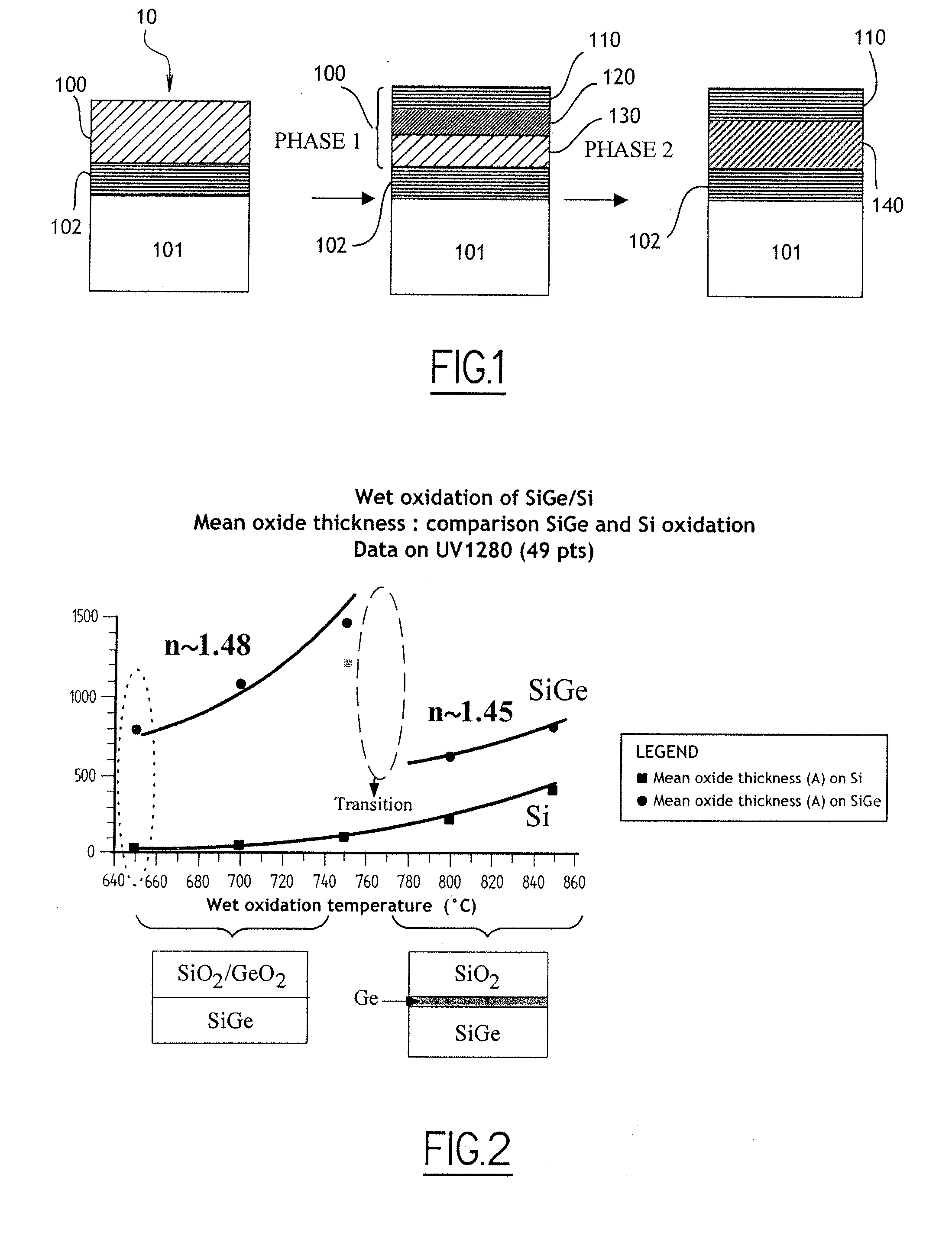
[0056] A first aspect of the invention is a method for oxidizing a surface region of a SiGe layer, the method comprising an oxidizing thermal treatment of the SiGe layer under an oxidizing atmosphere for oxidizing the surface region.

[0057] Such method comprises two phases: [0058] a first phase of oxidizing thermal treatment, which is carried out directly on the SiGe layer, and [0059] a second phase of high temperature annealing which is carried out on the SiGe layer after the first phase, in an inert atmosphere.

[0060] The first phase is carried out under an oxidizing atmosphere. It can be conducted as a dry thermal oxidation, or as a wet thermal oxidation.

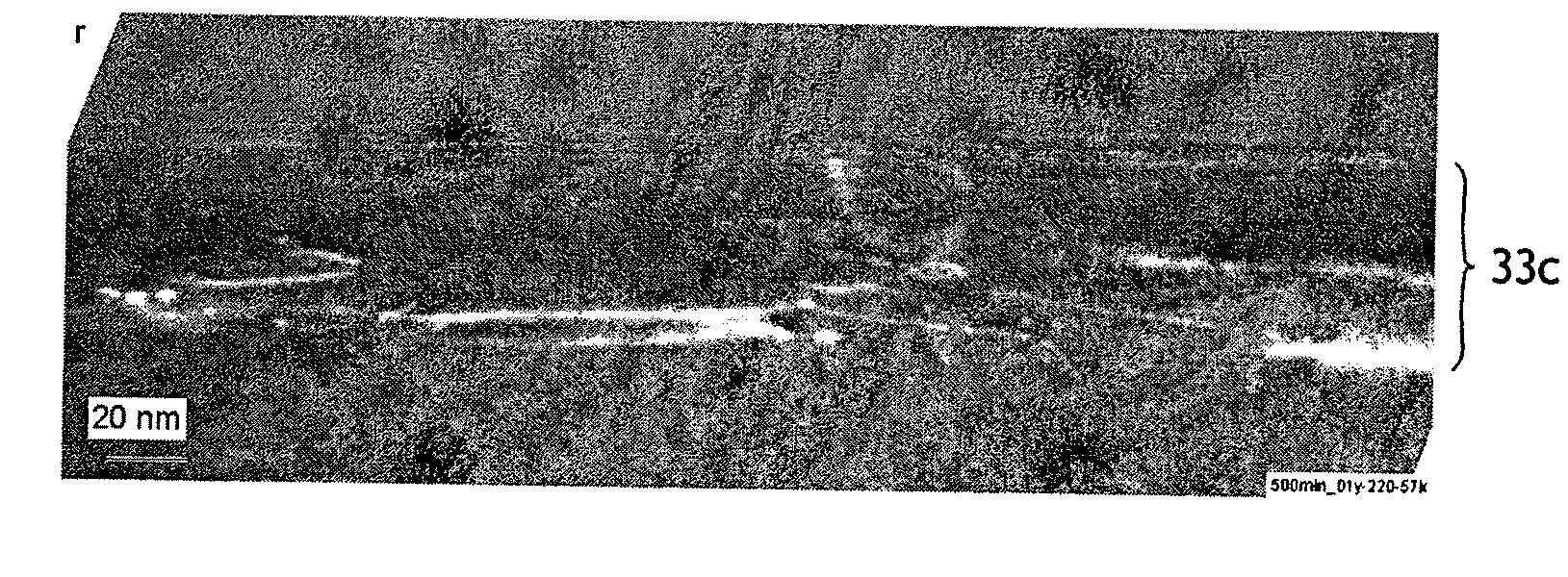
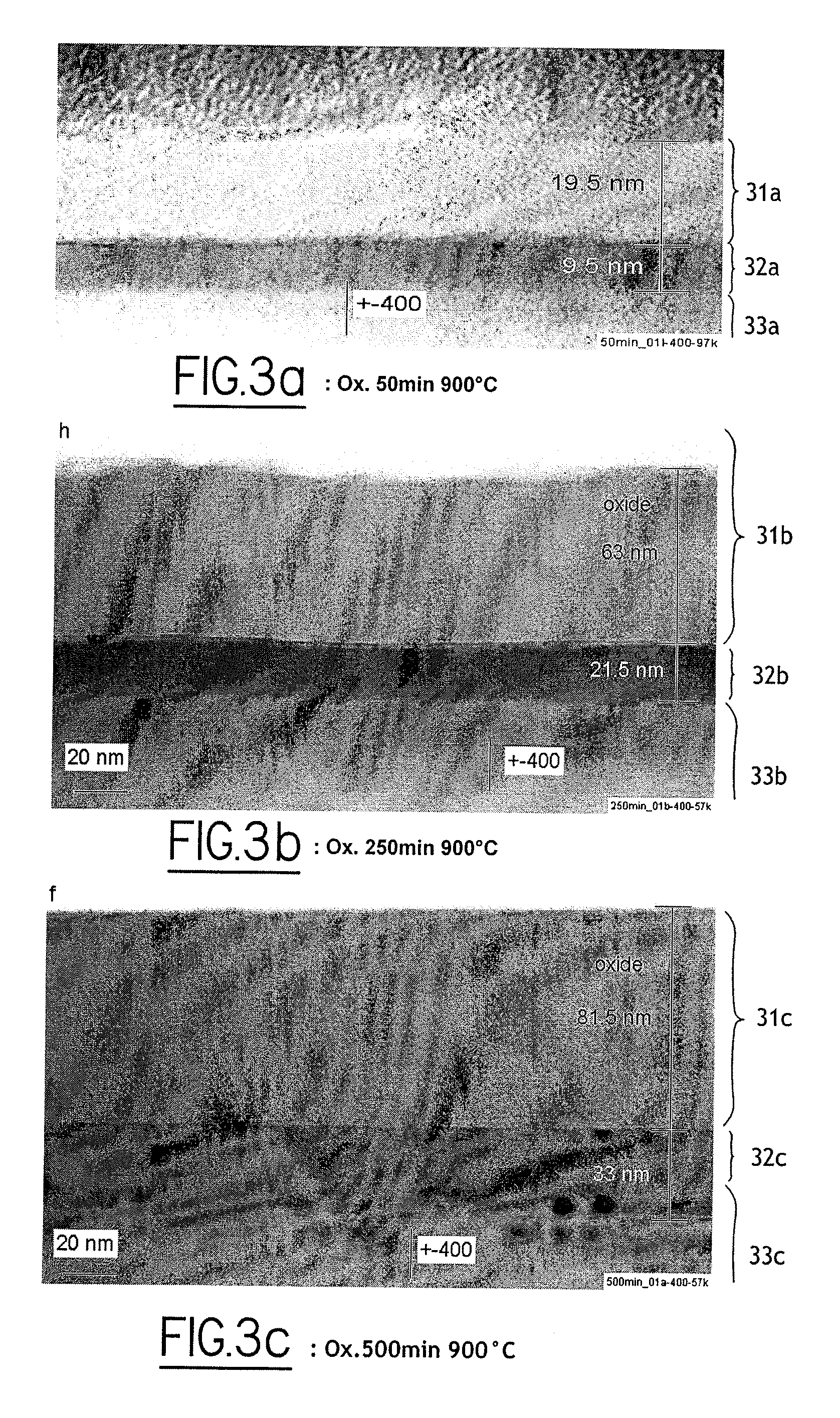
[0061] This first phase is carried out so as to obtain an oxidized region of the SiGe layer which is thick enough for forming a capping oxide which can protect the underlying SiGe from pitting during the subsequent second phase.

[0062] Moreover, this first phase is also carr...


PUM


Abstract

The invention concerns a method for oxidizing a surface region of a SiGe layer that includes an oxidizing thermal treatment of the SiGe layer for oxidizing the surface region. The method includes two phases—a first phase of oxidizing thermal treatment, carried out directly on the SiGe layer, so as to obtain an oxidized region which is thick enough for forming a capping oxide which can protect the underlying SiGe from pitting during the subsequent second phase, but thin enough for keeping the thickness of the oxidized surface region under a threshold thickness range, corresponding to the generation of dislocations within the SiGe layer; and—a second phase of high temperature annealing in an inert atmosphere which is carried out on the SiGe layer after the first phase. The SiGe layer is capped with the oxidized region created during the first phase, and the high temperature annealing allows the diffusion of Ge from a Ge-enriched region into the underlying part of the SiGe layer.

Description

CROSS-REFERENCE TO RELATED APPLICATIONS [0001] This application is a continuation of International application PCT / IB2005 / 000644 filed Feb. 24, 2005, the entire content of which is expressly incorporated herein by reference thereto.BACKGROUND [0002] The present invention concerns a method for oxidizing a surface region of a SiGe layer. It also concerns a method for treating a substrate comprising a semi-conducting layer on at least one of its surfaces, the method comprising an annealing of the substrate, the annealing itself comprising an oxidizing thermal treatment of the substrate under an oxidizing atmosphere for oxidizing a surface region of the substrate. [0003] Such methods already exist in general. The annealing of substrates as it is exposed above is typically carried out in a controlled atmosphere. Annealing in a non-oxidizing atmosphere (nitrogen, argon, vacuum, . . . ) usually has the drawback of causing a phenomenon known as pitting on the surface of a semiconductor laye...

Claims


Application Information

Patent Timeline
IPC IPC(8): H01L21/336H01L21/30
CPCH01L21/02126H01L21/02164H01L21/31658H01L21/02255H01L21/02236
Inventor DAVAL, NICOLAS
Owner S O I TEC SILICON ON INSULATOR THECHNOLOGIES
Why Eureka
Try Eureka