Organic light emitting display device and method of fabricating the same

a light-emitting display and organic technology, applied in the direction of solid-state devices, thermoelectric devices, meat/fish preservation, etc., can solve the problems of high transfer energy, open defects, and high aperture ratio, and achieve the effect of increasing (or maximizing) the transfer efficiency

Active Publication Date: 2007-11-08
SAMSUNG DISPLAY CO LTD
View PDF17 Cites 22 Cited by
  • Summary
  • Abstract
  • Description
  • Claims
  • Application Information

AI Technical Summary

Benefits of technology

[0020] An aspect of the present invention is directed to an organic light emitting display device which can increase (or maximize) transfer efficiency when an organic layer is formed by a laser induced thermal imaging (LITI) method and can prevent (or block) a short circuit between first and second electrodes, and a method of fabricating the same.

Problems solved by technology

If an organic light emitting display device including a pixel driving circuit is the bottom emission type, an aperture ratio is limited because the pixel driving circuit occupies a large area of a substrate of the organic light emitting display device.
Consequently, transfer energy becomes high, which may stimulate degradation of the organic layer, and the organic layer may not be properly transferred onto an edge part of the opening, which may result in an open defect.
However, in order to form the pixel defining layer thinly, the pixel defining layer is formed by spin coating, and thus uniformity or dispersion is poor.
As a result, an open defect may result around the via hole as illustrated with reference mark B. In addition, a protruding edge of a first electrode may not be fully covered, and may cause a short circuit between the first electrode and a second electrode.
Moreover, since the pixel defining layer formed of the organic material does not have a rigid layer characteristic, it may tear during removal of a transfer layer of a donor substrate after the organic layer is formed on an opening of the first electrode.
Thus, there is an additional possibility of a short circuit between the first and second electrodes.
However, as illustrated with reference mark C, the inorganic material has a poor ability to fill an inner via hole.
Also, if the layer is increased in thickness, cracks may occur around the via hole (reference mark D) and a protruding edge of the first electrode due to stress, and thus a short circuit between the first and second electrodes may still occur.

Method used


Image

  • Organic light emitting display device and method of fabricating the same
  • Organic light emitting display device and method of fabricating the same
  • Organic light emitting display device and method of fabricating the same

Examples


experimental example

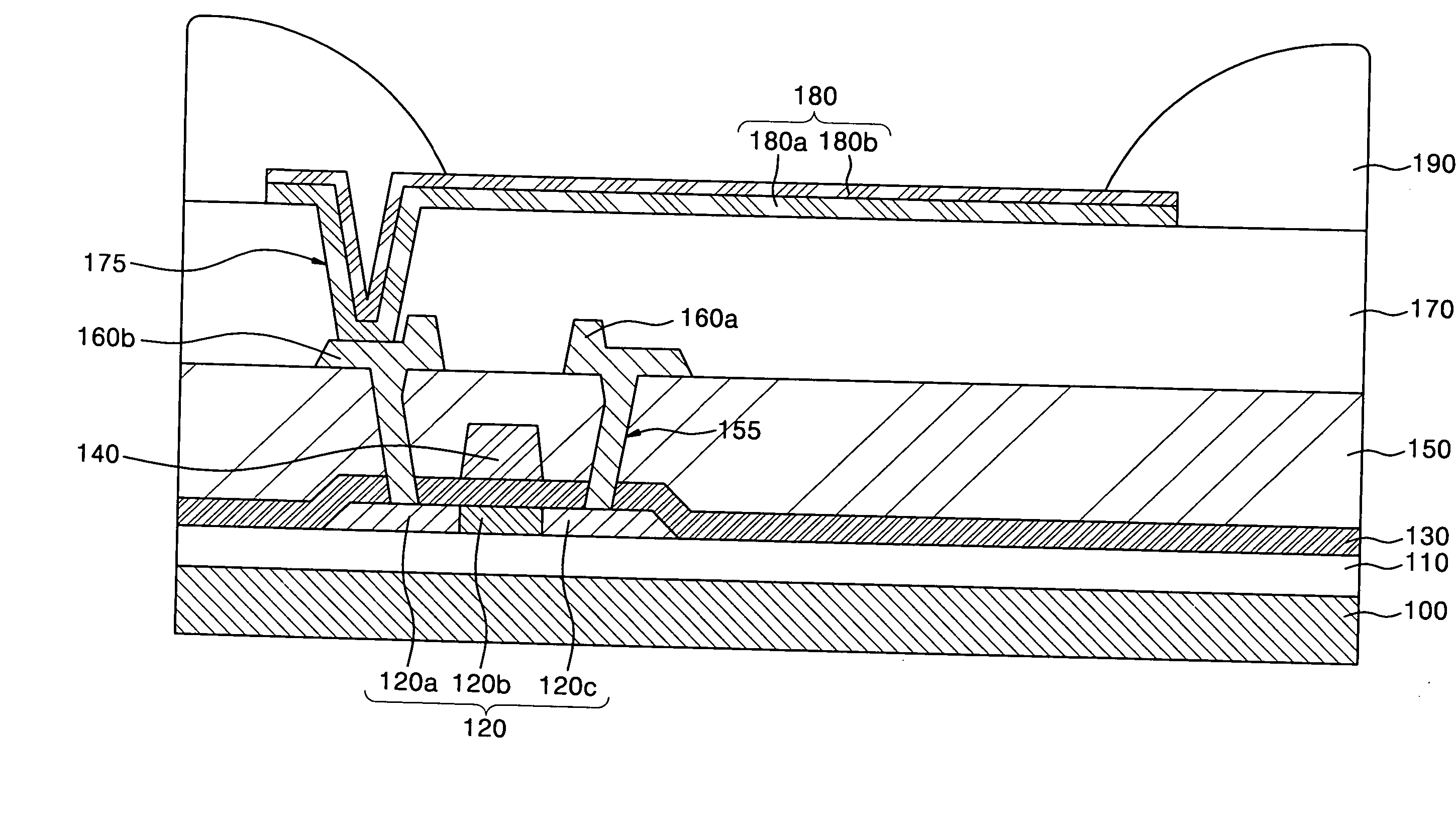
[0064] A planarization layer was formed to a thickness of 1 μm using SOG on a substrate having a substructure (which may be predetermined). A trench was formed to a thickness of about 1000 Å on the planarization layer, and a first electrode including a 1000 Å-thick reflective metal layer and a 70 Å-thick transparent conductive layer was formed to have opposite ends in the trench. A pixel defining layer was formed to a thickness of 2000 Å using polyimide on the first electrode. Then, the pixel defining layer was patterned so as to form an opening for exposing the first electrode.

[0065] An organic layer was formed by an LITI method in the opening. A second electrode was formed on the entire surface of the substrate including the organic layer, and thus an organic light emitting display device was completed.


PUM


Abstract

An organic light emitting display device and a method of fabricating the same are provided. A trench is formed in a planarization layer, and then a first electrode is formed to have opposite ends in the trench, thereby reducing a height difference between the planarization layer and the first electrode. That is, the thickness of a pixel defining layer formed on the first electrode may be reduced by reducing or minimizing protrusion of the first electrode with respect to the planarization layer. Thus, transfer efficiency can be increased when an organic layer is formed by a laser induced thermal imaging method, and reliability of a device can be improved by reducing or preventing thermal damage of the organic layer and open defects.

Description

CROSS-REFERENCE TO RELATED APPLICATION [0001] This application claims priority to and the benefit of Korean Patent Application No. 10-2006-0027661, filed Mar. 27, 2006, the entire content of which is incorporated herein by reference. BACKGROUND OF THE INVENTION [0002] 1. Field of the Invention [0003] The present invention relates to an organic light emitting display device and a method of fabricating the same. [0004] 2. Description of the Related Art [0005] An organic light emitting (or organic electroluminescence) display device is a type of flat panel display device. In more detail, the organic light emitting display device is an emissive display device that electrically excites an organic compound in order to emit light. Organic light emitting display devices do not need a backlight as is used in liquid crystal displays (LCDs), and thus may be made to be relatively lightweight and slim, and have a relatively simple structure. Also, organic light emitting display devices may be fa...

Claims


Application Information

Patent Timeline
Patent Type & Authority Applications(United States)
IPC IPC(8): H01L29/08
CPCH01L27/3246H01L51/5203H01L27/3258H10K59/122H10K59/124H10K59/805A23B4/031A23B4/005A23B4/01A23B7/02A23B7/01A23L3/40H10K50/805
Inventor IM, CHOONG-YOULYOO, KYUNG-JINJUN, WOO-SIKKWON, DO-HYUNKANG, TAE-WOOK
Owner SAMSUNG DISPLAY CO LTD
Why Eureka
Try Eureka