Memory circuit and method for refreshing dynamic memory cells

US20070258307A1Inactive Publication Date: 2007-11-08QIMONDA
5 Cites 3 Cited by

Patent Information

Authority / Receiving Office
US · United States
Current Assignee / Owner
Publication Date
2007-11-08
Estimated Expiration
Not applicable · inactive patent

Smart Images

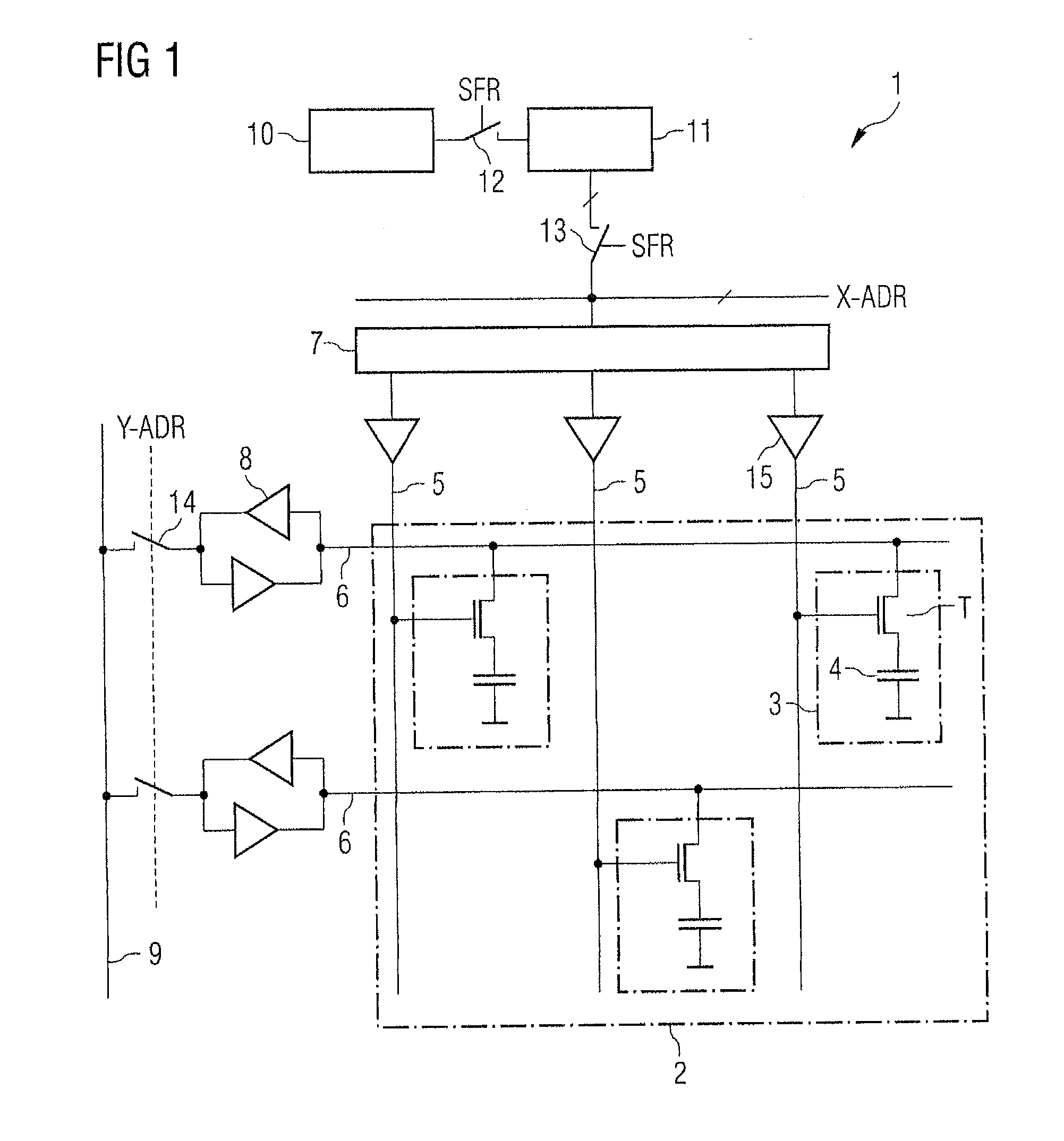
  • Figure 1
    Figure 1
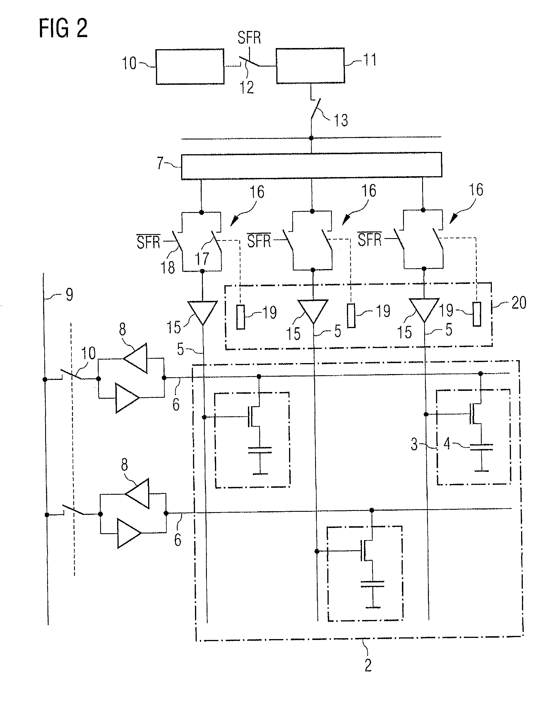
  • Figure 2
    Figure 2
  • Figure 3
    Figure 3
Patent Text Reader

Abstract

A memory circuit comprises a memory cell array with dynamic memory cells arranged on word lines and bit lines, a selection unit providing selection information and a refresh circuit selecting the memory cells in each case in dependence on the selection information and refreshing the selected memory cells so that any information stored therein is retained in each case.
Need to check novelty before this filing date? Find Prior Art

Description

CROSS-REFERENCE TO RELATED APPLICATIONS

[0001] This application claims foreign priority benefits under 35 U.S.C. § 119 to co-pending German patent application number DE 10 2006 020 098.5-55, filed 29 Apr. 2006. This related patent application is herein incorporated by reference in its entirety. BACKGROUND OF THE INVENTION

[0002] A memory cell array of a DRAM memory circuit has word lines and bit lines. In the case of a memory access, first one of the word lines is activated and, as a result, the memory cells arranged on the word line are in each case conductively connected to an associated bit line. During this process, a charge flows from a memory cell capacitance of the memory cell into the bit line. This leads to a deflection of the bit line voltage which can be detected with the aid of a read amplifier.

[0003] The memory cell capacitance of a dynamic memory chip is usually formed by means of a memory capacitor which is arranged in the substrate of the memory chip. However, a cha...

Examples

Embodiment Construction

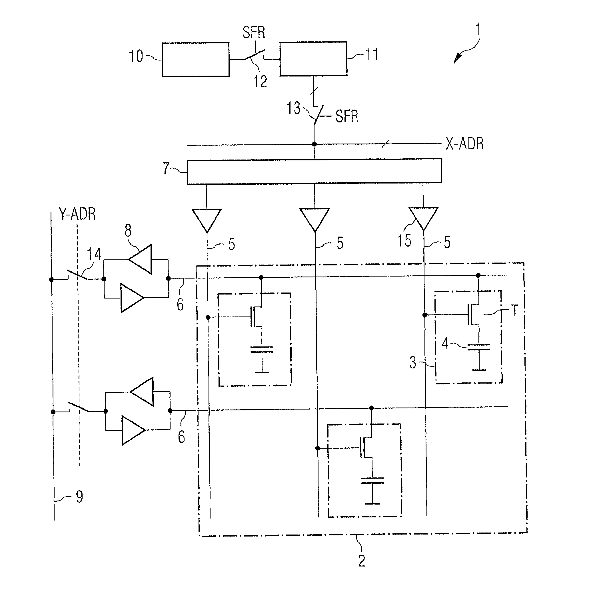
[0031]FIG. 1 shows a diagrammatic representation of a memory circuit 1 with a memory cell array 2. The memory cell array 2 comprises dynamic memory cells 3 in which an information item is in each case stored in the form of a charge in a capacitor 4. The memory cells 3 of the memory cell array 2 are arranged on word lines 5 and bit lines 6 so that, when one of the word lines 5 is activated, a corresponding selection transistor T of the memory cells 3 located on this word line is switched to conduct so that the charge flows to the corresponding bit line 6. The relevant word line 5 is selected by applying a word line address X-ADR to a word line decoder 7, which activates one of the word lines 5 in dependence on the word line address X-ADR via a corresponding word line driver 15 and leaves the other ones in the deactivated state. Each bit line 6 is connected to a read out amplifier 8 for amplifying the charge flowing from the addressed memory cell to the bit line 6 and outputting it to...