Dislocation-specific dielectric mask deposition and lateral epitaxial overgrowth to reduce dislocation density of nitride films

a dielectric mask and dislocation-specific technology, applied in the direction of basic electric elements, electrical apparatus, semiconductor devices, etc., can solve the problems of serious deformation of the performance of such laser diodes, affecting the subsequent device performance, and similar defects in other material systems, so as to inhibit the threading of the lattice mismatch

Inactive Publication Date: 2007-11-08
APPLIED MATERIALS INC
View PDF3 Cites 175 Cited by
  • Summary
  • Abstract
  • Description
  • Claims
  • Application Information

AI Technical Summary

Benefits of technology

[0008] In certain embodiments, the epitaxial nitride layer is formed on the substrate via MOCVD method comprising: introducing at least one nitrogen containing precursor into the reaction chamber; introducing a Group-III organo-metallic precursor and at least one etch compound into the reaction chamber, wherein the nitrogen-containing precursor reacts with the Group-III organo-metallic precursor to form a reaction mixture; and forming the epitaxial nitride layer on the substrate from the reaction mixture comprising the Group-III organo-metallic precursor and the nitrogen-containing precursor under conditions sufficient to allow preferential etching of the lattice mismatch dislocations of the epitaxial nitride layer during formation of the epitaxial nitride layer such that the etch pits are formed at the locations of the lattice mismatch dislocations while the epitaxial nitride layer is simultaneous grown within the etch pits to thereby inhibit threading of the lattice mismatch dislocations through the epitaxial nitride layer.

Problems solved by technology

The presence of defects in such wafer materials can seriously affect the subsequent device performance.
The performance of such laser diodes is seriously degraded by the presence of threading dislocations, which thread vertically through the epitaxial layers.
Similar defects are found in other material systems, for example, when GaAs is grown on SiGe / Si.
Another problem is that this approach requires considerable additional effort in processing and regrowth, requiring over 100 μm of epitaxial growth for best results.
This approach suffers from insufficient removal of defects.
This approach suffers from the use of very highly specialized and expensive equipment, and the production of rather small (˜1 cm2) GaN crystals.

Method used


Image

  • Dislocation-specific dielectric mask deposition and lateral epitaxial overgrowth to reduce dislocation density of nitride films
  • Dislocation-specific dielectric mask deposition and lateral epitaxial overgrowth to reduce dislocation density of nitride films
  • Dislocation-specific dielectric mask deposition and lateral epitaxial overgrowth to reduce dislocation density of nitride films

Examples


Embodiment Construction

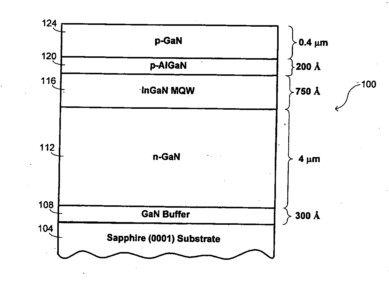
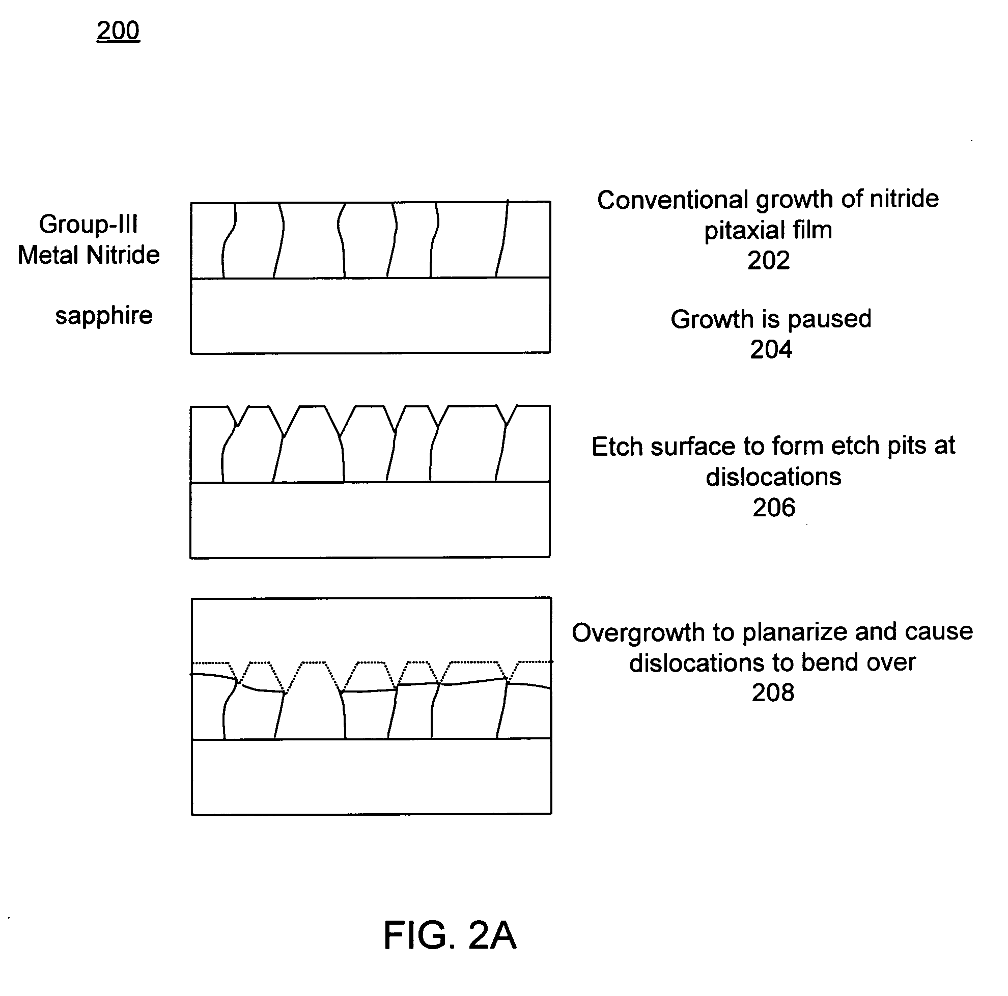
[0024] Nitride films may be deposited epitaxially by, e.g., MOVPE or MOCVD (Metal-Organic Vapor Phase Epitaxy or Metal-Organic Chemical Vapor Deposition), on sapphire, SiC, or Si substrates, for visible LEDs, near-UV laser diodes, and high power transistors. The performance of these devices is limited by the high dislocation density (˜109 cm−3) in the nitride layer, which arises from the large lattice mismatch (16% for the most common substrate, sapphire, and e.g., GaN) between the nitride film and substrate. For example, in light-emitting devices the dislocations represent extended non-radiative defects that serve to reduce the internal quantum efficiency; and also they are involved in device failure. In electronic devices, the presence of dislocations can cause failure or premature breakdown at high bias voltages.

[0025] As discussed above, several approaches have already been developed for reducing the dislocation density in nitride epitaxial films to improve their electronic and...


PUM

PropertyMeasurementUnit
diameteraaaaaaaaaa
temperatureaaaaaaaaaa
pressureaaaaaaaaaa

Abstract

In accordance with the present invention, improved methods for reducing the dislocation density of nitride epitaxial films are provided. Specifically, an in-situ etch treatment is provided to preferentially etch the dislocations of the nitride epitaxial layer to prevent threading of the dislocations through the nitride epitaxial layer. Subsequent to etching of the dislocations, an epitaxial layer overgrowth is performed. In certain embodiments, the etching of the dislocations occurs simultaneously with growth of the epitaxial layer. In other embodiments, a dielectric mask is deposited within the etch pits formed at the dislocations prior to the epitaxial layer overgrowth.

Description

CROSS-REFERENCES TO RELATED APPLICATIONS [0001] This application is related to the following copending, commonly assigned application, the entire disclosure of which is incorporated herein by reference for all purposes: U.S. application Ser. No. ______, Attorney Docket Number A11024 / T71600, entitled “DISLOCATION-SPECIFIC LATERAL EPITAXIAL OVERGROWTH TO REDUCE DISLOCATION DENSITY OF NITRIDE FILMS.”BACKGROUND OF THE INVENTION [0002] Epitaxial wafer materials are widely used as starting materials in semiconductor device fabrication. The presence of defects in such wafer materials can seriously affect the subsequent device performance. For example, GaN and its related compounds InGaN and AlGaN are widely used in the fabrication of short-wavelength semiconductor laser diodes. The performance of such laser diodes is seriously degraded by the presence of threading dislocations, which thread vertically through the epitaxial layers. Similar defects are found in other material systems, for ex...

Claims


Application Information

Patent Timeline
Patent Type & Authority Applications(United States)
IPC IPC(8): H01L21/00
CPCH01L21/0242H01L21/02458H01L21/0254H01L33/007H01L21/02647H01L21/0265H01L21/02639
Inventor BOUR, DAVIDNIJHAWA, SANDEEPSMITH, JACOBWASHINGTON, LORI
Owner APPLIED MATERIALS INC
Why Eureka
Try Eureka