
Dislocation-specific lateral epitaxial overgrowth to reduce dislocation density of nitride films
a nitride film and dislocation density technology, applied in the direction of crystal growth process, polycrystalline material growth, chemically reactive gases, etc., can solve the problems of serious deformation of the performance of such laser diodes, similar defects in other material systems, and serious affecting the subsequent device performance. , to achieve the effect of reducing the dislocation density of nitride epitaxial layers and reducing the dislocation density of a nitride semiconductor structur
- Summary
- Abstract
- Description
- Claims
- Application Information
AI Technical Summary
Benefits of technology
Problems solved by technology
Method used
Image

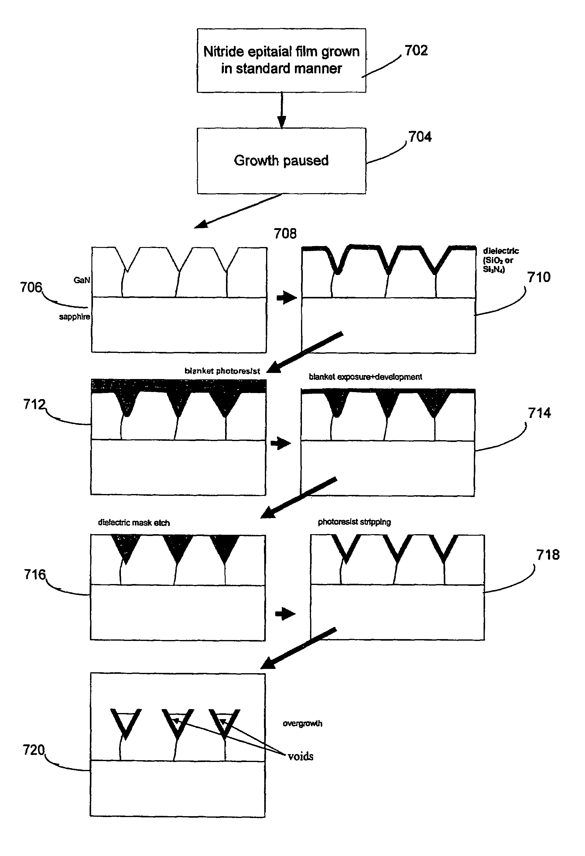
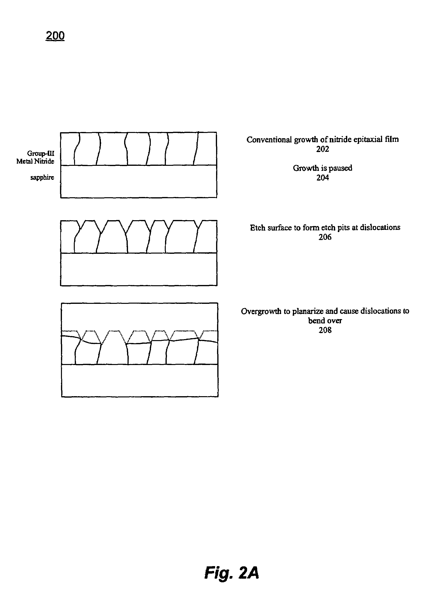
Examples
Embodiment Construction
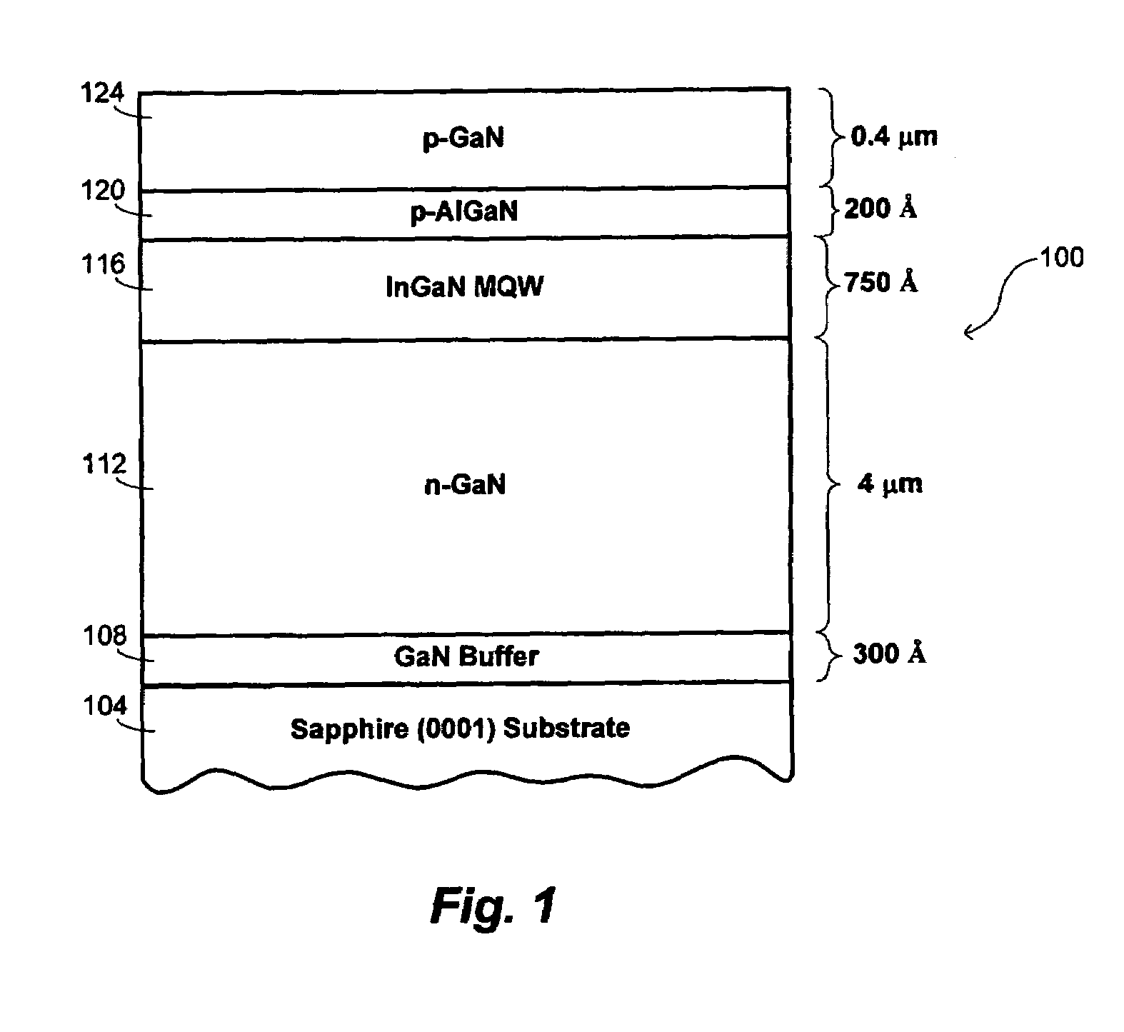
[0024]Nitride films may be deposited epitaxially by, e.g., MOVPE or MOCVD (Metal-Organic Vapor Phase Epitaxy or Metal-Organic Chemical Vapor Deposition), on sapphire, SiC, or Si substrates, for visible LEDs, near-UV laser diodes, and high power transistors. The performance of these devices is limited by the high dislocation density (˜109 cm−3) in the nitride layer, which arises from the large lattice mismatch (16% for the most common substrate, sapphire, and e.g., GaN) between the nitride film and substrate. For example, in light-emitting devices the dislocations represent extended non-radiative defects that serve to reduce the internal quantum efficiency; and also they are involved in device failure. In electronic devices, the presence of dislocations can cause failure or premature breakdown at high bias voltages.
[0025]As discussed above, several approaches have already been developed for reducing the dislocation density in nitride epitaxial films to improve their electronic and op...
PUM
| Property | Measurement | Unit |
|---|---|---|
| thickness | aaaaa | aaaaa |
| thickness | aaaaa | aaaaa |
| diameter | aaaaa | aaaaa |
Abstract
Description
Claims
Application Information