Plasma display panel and manufacturing method thereof
- Summary
- Abstract
- Description
- Claims
- Application Information
AI Technical Summary
Benefits of technology
Problems solved by technology
Method used
Image

Examples
Embodiment Construction
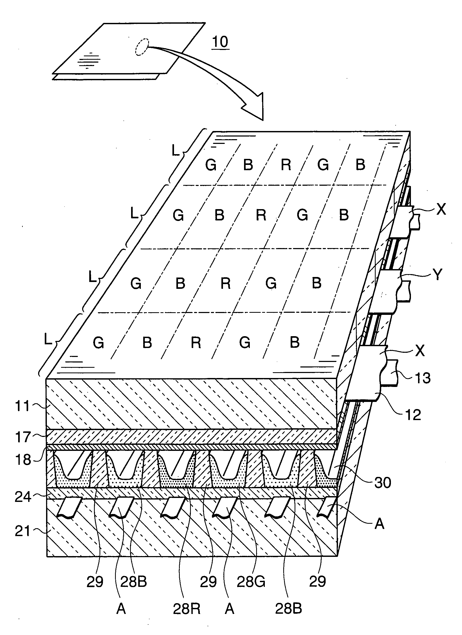
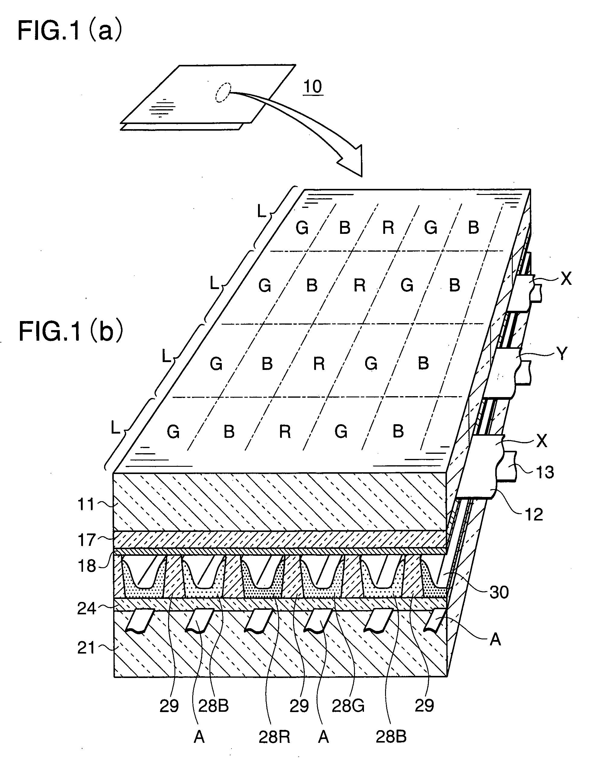
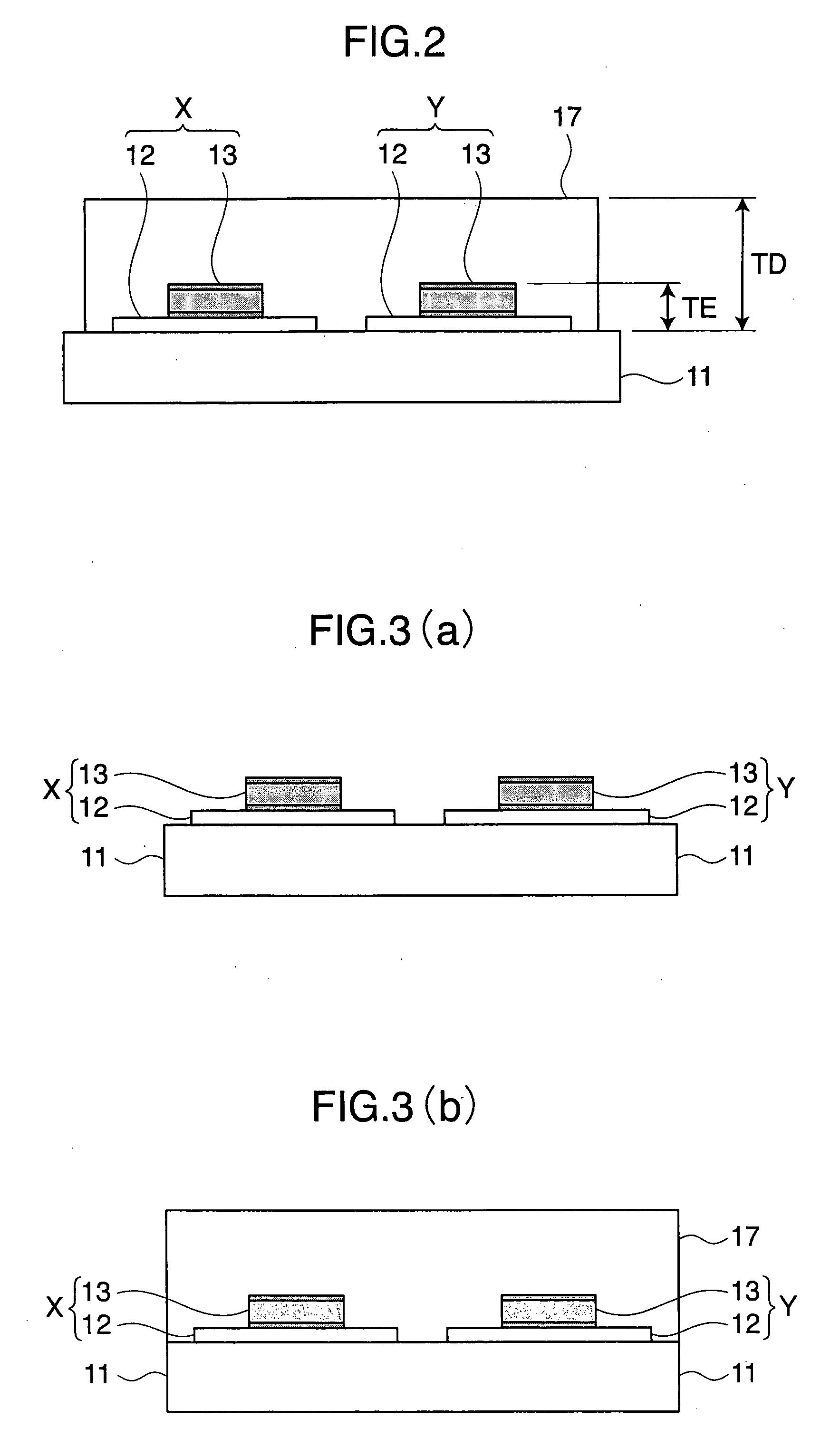
[0024]In the present invention, examples of the substrate include substrates of materials such as glass, quartz and ceramics, as well as any of these substrates on which a desired structure such as electrodes, an insulating film, a dielectric layer, a protective film and the like are formed.
[0025]A plurality of metal electrodes may be formed on the substrate in a predetermined direction. These metal electrodes can be formed by using various known materials through known methods in the corresponding field. With respect to the materials used for the electrodes, examples thereof include metal conductive materials such as Ag, Au, Al, Cu and Cr. With respect to the forming method of the electrodes, various conventionally known methods in the corresponding field may be used. For example, a thick-film forming technique such as printing may be used to form the electrodes, or a thin-film forming technique corresponding to a physical deposition method or a chemical deposition method may be us...
PUM
 Abstract
Description
Claims
Application Information
 - Generate Ideas
- Intellectual Property
- Life Sciences
- Materials
- Tech Scout
- Unparalleled Data Quality
- Higher Quality Content
- 60% Fewer Hallucinations
Browse by: Latest US Patents, China's latest patents, Technical Efficacy Thesaurus, Application Domain, Technology Topic, Popular Technical Reports.
© 2025 PatSnap. All rights reserved.Legal|Privacy policy|Modern Slavery Act Transparency Statement|Sitemap|About US| Contact US: help@patsnap.com