Liquid crystal display having defect repair mechanism

a liquid crystal display and defect repair technology, applied in non-linear optics, instruments, optics, etc., can solve the problem of image displaying quality degraded liquid crystal display, and achieve the effect of improving the display quality of liquid crystal display devices and high pixel defects

Inactive Publication Date: 2007-11-15
SAMSUNG DISPLAY CO LTD
View PDF7 Cites 29 Cited by
  • Summary
  • Abstract
  • Description
  • Claims
  • Application Information

AI Technical Summary

Benefits of technology

[0014]According to the above, each pixel unit has a repair electrode branching from a gate line and overlapped with the pixel electrode, so that a turn-off or pulsed repair voltage can be applied to the pixel electrode of a pixel area where a high pixel defect occurs after a repair-activating process is carried out (i.e., by laser activation). Accordingly, the high pixel defect appears to be removed, so the display quality of the liquid crystal display device can be improved.

Problems solved by technology

When an LCD has one or more such high pixel defects, the image displaying quality of the liquid crystal display is considered degraded.

Method used


Image

  • Liquid crystal display having defect repair mechanism
  • Liquid crystal display having defect repair mechanism
  • Liquid crystal display having defect repair mechanism

Examples


Embodiment Construction

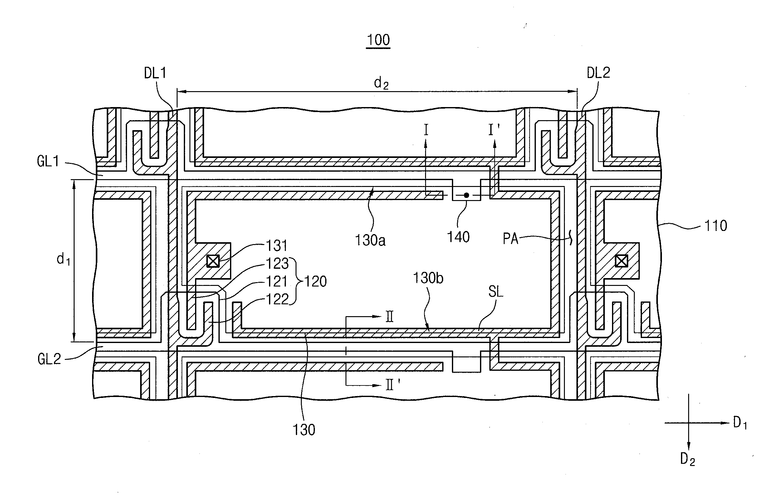
[0024]FIG. 1 is a layout view showing a transistor-array substrate 100 according to an exemplary embodiment of the present invention. Although the transistor-array substrate 100 includes a plurality of pixels, since each of the pixels has substantially the same structure, detailed description about only one pixel will be made below.

[0025]Referring to FIG. 1, the transistor-array substrate 100 includes an insulative base substrate 110, first and second gate lines GL1 and GL2, first and second data lines DL1 and DL2, a thin film transistor (TFT) 120, a pixel electrode 130, a storage line SL, and a repair electrode 140. The first illustrated gate line GL1 is operatively coupled to the gate of the TFT of a next adjacent stage. The second illustrated gate line GL2 is operatively coupled to the gate 121 of TFT 120. The right side data line DL2 is operatively coupled to the source of the TFT in the next adjacent stage. The left side, first data line DL1 is operatively coupled to the source...


PUM

PropertyMeasurementUnit
pixel-off voltageaaaaaaaaaa
areaaaaaaaaaaa
common voltageaaaaaaaaaa

Abstract

A liquid crystal display that is subject to pixel-high defects due to manufacturing anomalies is provided with programmable repair means for each pixel electrode. In one embodiment, a transistor-array substrate is provided with plural gate lines that are separated from each other by a first interval, plural data lines that are insulated from the gate lines while crossing the gate lines, and separated from each other by a second interval larger than the first interval, thereby defining plural pixel areas. Each pixel area has a corresponding pixel unit comprising a switching device, pixel electrode, and repair electrode. The repair electrode branches from a neighboring gate line and extends such that the repair electrode is in overlapping spaced-apart relation with the pixel electrode and selectively connectable to the pixel electrode. Accordingly, a pixel where a high pixel defect occurs can be repaired by selective connection with the repair electrode, thereby improving display quality of the liquid crystal display.

Description

CROSS-REFERENCE TO RELATED APPLICATION[0001]This application relies for priority upon Korean Patent Application No. 2006-43074 filed on May 12, 2006, the disclosure of which is incorporated herein by reference.BACKGROUND[0002]1. Field of Invention[0003]The present disclosure of invention relates to liquid crystal displays (LCD's) and more particularly to LCD's which are subject to manufacturing defects that can result in creation of always-on or always-white pixel areas.[0004]2. Description of the Related Art[0005]A typical liquid crystal display (LCD) has a sandwich like structure that includes a transistor-array substrate, a color-filter substrate, and a liquid crystal layer interposed between the transistor-array substrate and the color-filter substrate.[0006]The transistor-array substrate typically includes a plurality of gate lines, a plurality of data lines and a plurality of pixel areas that are defined by intersections the gate lines and the data lines. A plurality of pixel ...

Claims


Application Information

Patent Timeline
Patent Type & Authority Applications(United States)
IPC IPC(8): G02F1/1333
CPCG02F1/136213G02F1/136286G02F1/136259G02F1/1343
Inventor KIM, BEOM-JUNLEE, JONG-HWANJEON, SANG-JINKIM, SUNG-MANLEE, BONG-JUNLEE, HONG-WOO
Owner SAMSUNG DISPLAY CO LTD
Why Eureka
Try Eureka