Precharge circuit of semiconductor memory apparatus

a technology of pre-charge circuit and semiconductor memory, which is applied in the direction of static storage, digital storage, instruments, etc., can solve the problems of consuming a large amount of current, conventional pre-charge circuit of semiconductor memory apparatus, and inability to supply a sufficient amount of current to the plurality of local input/output lines lio and liob, so as to reduce the current burden of the core voltage

Inactive Publication Date: 2007-11-15
SK HYNIX INC
View PDF5 Cites 11 Cited by
  • Summary
  • Abstract
  • Description
  • Claims
  • Application Information

AI Technical Summary

Benefits of technology

[0027]Embodiments of the present invention provide a precharge circuit of a semiconductor memory apparatus that uses a core voltage and a first supply voltage as precharge power supplies for a pair of local input / output lines so as to reduce the current burden of the core voltage.

Problems solved by technology

In many semiconductor memory apparatuses, a plurality of pairs of local input / output lines LIO and LIOb are precharged simultaneously, thus consuming a large amount of current.
A conventional precharge circuit of the semiconductor memory apparatuses, however, is unable to supply a sufficiently large amount of current to the plurality of the pairs of local input / output lines LIO and LIOb, since the internally generated core voltage VCORE1 is not responsive enough to simultaneously supply such large amount of current.
Further, when the core voltage VCORE1 drops, the precharge level is also lowered, causing deterioration in the performance of the sense amplifier S / A, which is designed to operate in a state wherein the pairs of local input / output lines LIO and LIOb are fully precharged to the level of the core voltage VCORE1.

Method used


Image

  • Precharge circuit of semiconductor memory apparatus
  • Precharge circuit of semiconductor memory apparatus
  • Precharge circuit of semiconductor memory apparatus

Examples


Embodiment Construction

[0049]Embodiments of the present invention will now be described in detail with reference to the accompanying drawings.

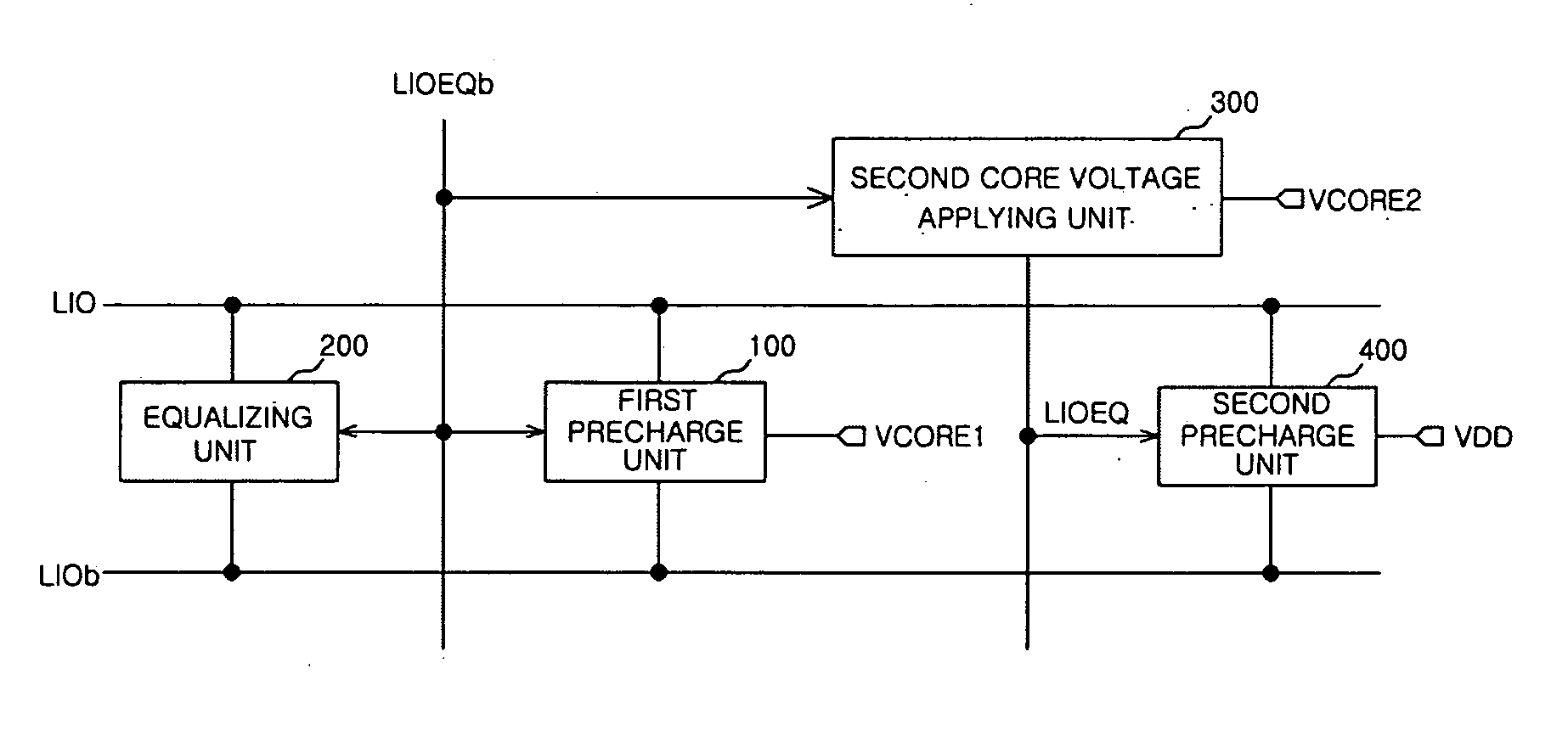
[0050]Referring to FIG. 4, the precharge circuit of a semiconductor memory apparatus according to an embodiment of the present invention includes a first precharge unit 100, an equalizing unit 200, a second core voltage applying unit 300 and a second precharge unit 400.

[0051]The first precharge unit 100 applies a first core voltage VCORE1 to a pair of local input / output lines LIO and LIOb, in response to a first precharge signal LIOEQb, to precharge the pair of local input / output lines LIO and LIOb.

[0052]The equalizing unit 200 equalizes the pair of local input / output lines LIO and LIOb in response to the first precharge signal LIOEQb.

[0053]The second core voltage applying unit 300 outputs a second precharge signal LIOEQ in response to the first precharge signal LIOEQb.

[0054]The second precharge unit 400 applies a clamp voltage generated using a first supply voltage...


PUM


Abstract

Disclosed is a precharge circuit of a semiconductor apparatus. The precharge circuit of a semiconductor memory apparatus includes a first precharge unit and a second precharge unit. The first precharge unit applies a first core voltage to a pair of local input/output lines, in response to a first precharge signal, to precharge the pair of local input/output lines. The second precharge unit applies a clamp voltage, which is generated using a first supply voltage, to the pair of local input/output lines, in response to the first precharge signal, to precharge the pair of local input/output lines.

Description

BACKGROUND OF THE INVENTION[0001]1. Technical Field[0002]The present invention relates to a precharge circuit of a semiconductor memory apparatus, and more particularly, to a precharge circuit of a semiconductor memory apparatus that precharges a pair of local input / output lines LIO and LIOb.[0003]2. Related Art[0004]A conventional precharge circuit of a semiconductor memory apparatus will now be described with reference to FIGS. 1 to 3.[0005]FIG. 1 is a circuit diagram of a conventional precharge circuit of a semiconductor memory apparatus.[0006]The conventional precharge circuit of a semiconductor memory apparatus includes a first PMOS transistor P1, a second PMOS transistor P2 and a third PMOS transistor P3.[0007]The first PMOS transistor P1 and a second PMOS transistor P2 precharge a pair of local input / output lines LIO and LIOb to a core voltage VCORE1 in response to a precharge signal LIOEQb.[0008]The third PMOS transistor P3 equalizes the pair of local input / output lines LIO ...

Claims


Application Information

Patent Timeline
Patent Type & Authority Applications(United States)
IPC IPC(8): G11C7/00
CPCG11C7/1048G11C7/02G11C7/12
Inventor LEE, JONG CHERN
Owner SK HYNIX INC
Why Eureka
Try Eureka