Display substrate and method of manufacturing the same and liquid crystal display apparatus having the same

a technology of liquid crystal display apparatus and display substrate, which is applied in the direction of instruments, semiconductor devices, optics, etc., can solve the problems of deterioration of the reliability of the lcd apparatus, and achieve the effect of reducing the number of display substrate defects

Inactive Publication Date: 2007-11-22
SAMSUNG ELECTRONICS CO LTD
View PDF4 Cites 32 Cited by
  • Summary
  • Abstract
  • Description
  • Claims
  • Application Information

AI Technical Summary

Benefits of technology

[0014]According to the above, an application of static electricity generated in a manufacturing process of a display substrate is prevented, so that defects of the display substrate may decrease.

Problems solved by technology

The static electricity flowing into the pixel substrate causes a wiring defect such as a disconnection and a circuit short of the wirings and damages the thin film transistor, so that reliability of LCD apparatus is deteriorated.

Method used


Image

  • Display substrate and method of manufacturing the same and liquid crystal display apparatus having the same
  • Display substrate and method of manufacturing the same and liquid crystal display apparatus having the same
  • Display substrate and method of manufacturing the same and liquid crystal display apparatus having the same

Examples


first embodiment

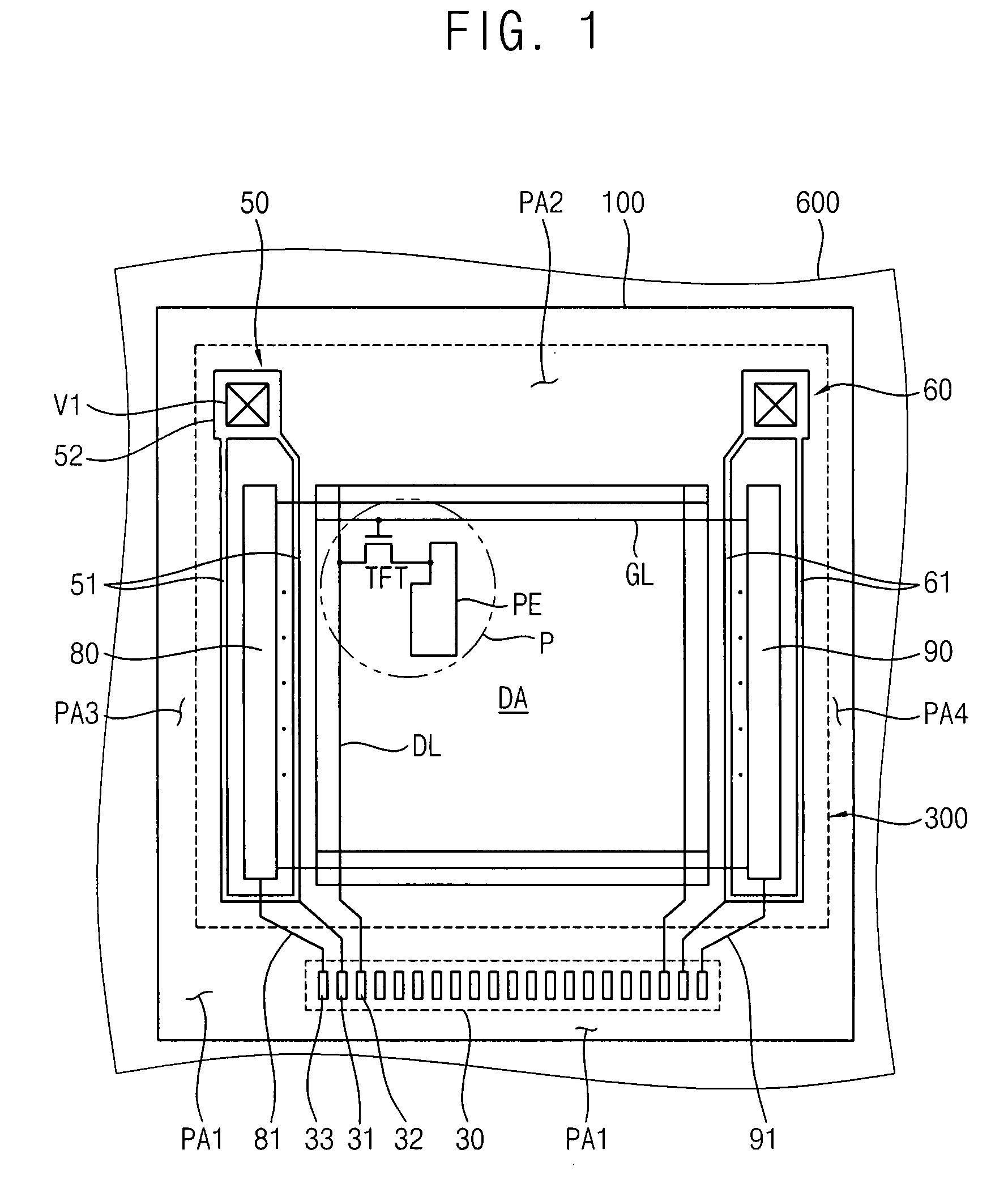
[0029]FIG. 1 is a plan view illustrating an LCD apparatus 600 in accordance with the present invention.

[0030]Referring to FIG. 1, an LCD apparatus 600 includes a display substrate 100, an opposing substrate 300 and a liquid crystal layer (not shown) disposed between the display substrate 100 and the opposing substrate 300.

[0031]The display substrate 100 includes a first transparent substrate. A display area DA, a first peripheral area PA1, a second peripheral area PA2, a third peripheral area PA3 and a fourth peripheral area PA4 surrounding the display area DA are defined on the first transparent substrate. The first, second, third and fourth peripheral areas PA1, PA2, PA3 and PA4 surround the display area DA.

[0032]A plurality of gate wirings GL, a plurality of source wirings DL, and a plurality of pixel portions P defined by the gate wirings GL and the source wirings DL are formed in the display area DA. A thin film transistor TFT electrically connected to each of the gate wirings ...

second embodiment

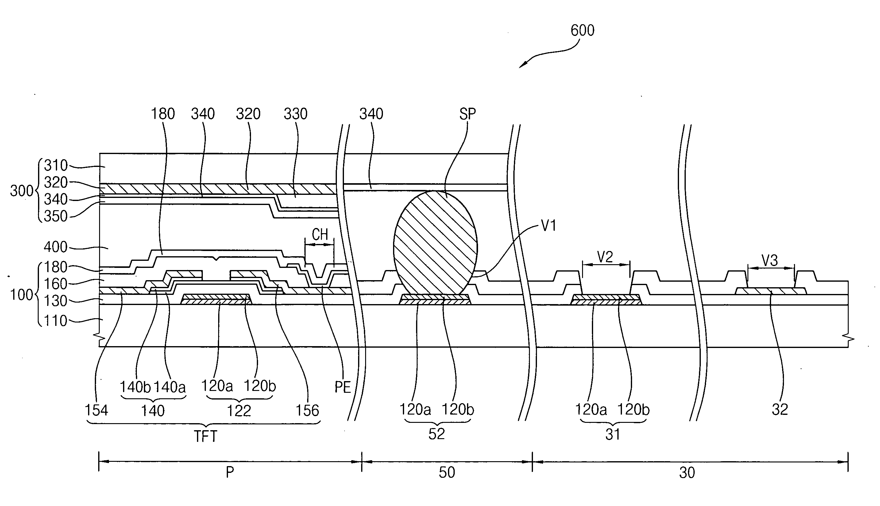
[0101]FIG. 10 is a cross-sectional view illustrating a display substrate in accordance with the present invention.

[0102]The display substrate 700 of the present embodiment of the present invention has a number of structures which are common to the first embodiment. Thus, the same reference numerals are used to refer to the same or like parts as those described in the first embodiment and any further repetitive explanation concerning the above elements are not provided.

[0103]Referring to FIGS. 1, 2 and 10, the first and second common voltage wirings 51 and 61 and the electrical short pad 52 may be formed from the gate pattern in FIGS. 1 and 2. However, the first and second common voltage wirings 51 and 61 and the electrical short pad 52-1 as shown in FIG. 10, may be formed from substantially the same source pattern as the source wiring DL from which source electrode 154 extends. The source pattern includes a third metallic layer having greater ionization energy than the first metalli...

third embodiment

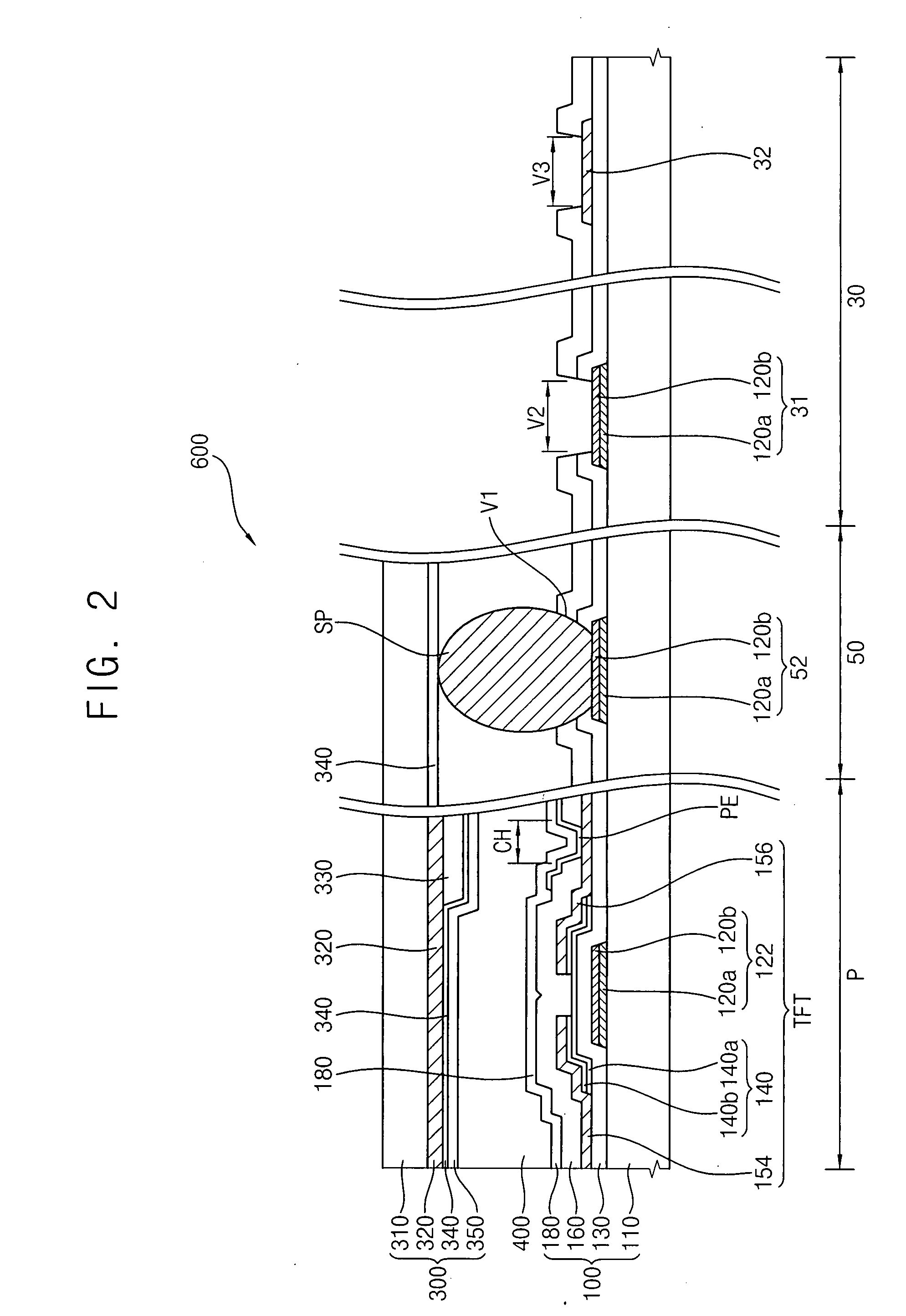
[0104]FIG. 11 is a cross-sectional view illustrating a display substrate in accordance with the present invention.

[0105]The display substrate 800 of the present embodiment of the present invention has a number of structures which are common to the first embodiment. Thus, the same reference numerals are used to refer to the same or like parts as those described in the first embodiment and any further repetitive explanation concerning the above elements are not provided.

[0106]Referring to FIGS. 2 and 11, electrical short pad 52 of a display substrate 800 of the third embodiment of the present invention includes a first metallic layer 120a of a gate pattern, a second metallic layer 120b of the gate pattern and a third metallic layer 150 of a source pattern. The first, second and third metallic layers 120a, 120b and 150 are formed on a first transparent substrate 110, in sequence. The third metallic layer 150 contacts the second metallic layer 120b through a first via hole V1 formed in ...


PUM

PropertyMeasurementUnit
areaaaaaaaaaaa
ionization energyaaaaaaaaaa
electrically conductiveaaaaaaaaaa

Abstract

A display substrate includes a plurality of gate wirings, a plurality of source wirings, a plurality of pixel portions, an electrical short pad part and a short element. The electrical short pad part is formed in a peripheral area surrounding the display area and formed from at least one of the gate metallic layer and the source metallic layer to receive a common voltage. The short element makes contact with the electrical short pad part and has electric conductivity. The electrical short pad part includes a first metallic layer and a second metallic layer in sequence, and the second metallic layer has greater ionization energy than the first metallic layer. The electrical short pad part is exposed onto the surface of the display substrate. Accordingly, an extra cover electrode for preventing the electrical short pad part from corrosion may be omitted, so that static electricity is prevented from being applied into the display substrate.

Description

CROSS-REFERENCE TO RELATED APPLICATIONS[0001]This application relies for priority upon Korean Patent Application No. 10-2006-45021 filed on May 19, 2006, the contents of which are herein incorporated by reference in its entirety.BACKGROUND OF THE INVENTION[0002]1. Field of the Invention[0003]The present invention relates to a display substrate and a method of manufacturing the display substrate and a liquid crystal display apparatus having the display substrate. More particularly, the present invention relates to a display substrate and a method of manufacturing the display substrate and a liquid crystal display apparatus having the display substrate for decreasing defects.[0004]2. Description of the Related Art[0005]In general, a liquid crystal display (LCD) apparatus includes a pixel substrate, an opposite substrate opposite to the pixel substrate and a liquid crystal layer disposed between the pixel substrate and the opposite substrate. Liquid crystal molecules of the liquid crys...

Claims


Application Information

Patent Timeline
Patent Type & Authority Applications(United States)
IPC IPC(8): G02F1/1345
CPCG02F1/13452G02F1/136204H01L27/124G02F2001/13456H01L29/4908G02F2001/133388G02F1/133388G02F1/13456G02F1/1345
Inventor OH, JEONG-MINLEE, IN-SUNGYUM, HO-NAM
Owner SAMSUNG ELECTRONICS CO LTD
Why Eureka
Try Eureka