
Memory cell array, method of producing the same, and semiconductor memory device using the same

a memory cell array and memory cell technology, applied in the field of memory cell arrays, can solve the problems of difficult connection of electrodes located at the bottom of the 3-dimensional region of semiconductor to common interconnection lines such as bit lines or word lines, and the production process of memory cells each composed of one mosfet and one capacitor is complicated, and the production process is not good in compatibility with the logic circuit production process

Active Publication Date: 2007-12-06
FUJITSU LTD
View PDF2 Cites 160 Cited by
  • Summary
  • Abstract
  • Description
  • Claims
  • Application Information

AI Technical Summary

Benefits of technology

[0006] The vertical double-gate transistor refers to a MOSFET configured such that a 3-dimensional isolated region of silicon (Si) is formed on a supporting substrate and a MOSFET having two gate electrodes is formed in this 3-dimensional isolated region of silicon (Si) such that one gate electrode is formed on one side surface thereof and the other one is formed on the opposite side surface. In the vertical double-gate transistor having such a structure, because the channel of the MOSFET is controlled using the two gate electrodes, a reduction in a current flowing between the source and drain in a waiting state can be achieved. Thus, use of the vertical double-gate transistor structure makes it possible to solve problems caused by reduction in size of MOSFETs.
[0018] In a third aspect of the present invention, there is provided a memory cell array including semiconductor regions formed in the shape of a lattice on a supporting insulating substrate, a plurality of memory cells formed in the respective semiconductor regions in the form of an array, insulating regions formed between adjacent semiconductor regions so as to insulate the memory cells, front gate lines, back gate lines, bit lines, and source lines. Each memory cell includes a source region formed on the top surface of a semiconductor region at an intersection of the lattice, a drain region formed on the top surface the semiconductor region at the intersection of the lattice, a front gate region formed on a gate insulating film formed on a first side surface of the semiconductor region such that the source region and the drain region are separated from each other by the front gate region, and a back gate region formed on a gate insulating film formed on a second side surface of the semiconductor region, the second side surface being located opposite to the first side surface, the back gate region being formed such that the source region and the drain region are separated from each other by the back gate region. Each memory cell shares the source region or the drain region with a memory cell adjacent in the column direction. Each memory cell also shares the front gate region or the back gate region with a memory cell adjacent in the row direction. Each front gate line extends in the column direction and connects together front gate regions of memory cells in respective semiconductor regions located in one column. Each back gate line extends in the row direction and connects together hack gate regions of respective memory cells located in one row. Each bit line extends in the column direction and connects together drain regions of memory cells in respective semiconductor regions located in one column. Each source line extends in the row direction and connects together source regions formed on the top of semiconductor regions of respective memory cells located in one row, the source regions being located along a lattice line extending in the row direction.
[0006] The vertical double-gate transistor refers to a MOSFET configured such that a 3-dimensional isolated region of silicon (Si) is formed on a supporting substrate and a MOSFET having two gate electrodes is formed in this 3-dimensional isolated region of silicon (Si) such that one gate electrode is formed on one side surface thereof and the other one is formed on the opposite side surface. In the vertical double-gate transistor having such a structure, because the channel of the MOSFET is controlled using the two gate electrodes, a reduction in a current flowing between the source and drain in a waiting state can be achieved. Thus, use of the vertical double-gate transistor structure makes it possible to solve problems caused by reduction in size of MOSFETs.

Problems solved by technology

However, SRAMs have a limit in reduction in size.
On the other hand, DRAMs including memory cells each composed of one MOSFET and one capacitor need a complicated production process and is not good in compatibility with the production process of logic circuits.
However, when memory cells each including a vertical double-gate transistor are disposed in the form of an array, the following problems can occur.
When drain regions, source regions, first side-surface gate electrodes, and second side-surface gate electrodes of vertical double-gate transistors in respective memory cells are connected by common interconnection lines extending in row and column directions, it is difficult to connect electrodes located at the bottom of 3-dimensional regions of semiconductor to common interconnection lines such as bit lines or word lines.
If isolation regions are simply disposed between adjacent memory cells to electrically isolate drain regions, source regions, first side-surface electrodes, and second side-surface electrodes of respective memory cells, the result is an increase in the total area of the array, and it is difficult to realize a high-density memory cell array.

Method used


Image

  • Memory cell array, method of producing the same, and semiconductor memory device using the same
  • Memory cell array, method of producing the same, and semiconductor memory device using the same
  • Memory cell array, method of producing the same, and semiconductor memory device using the same

Examples


first embodiment

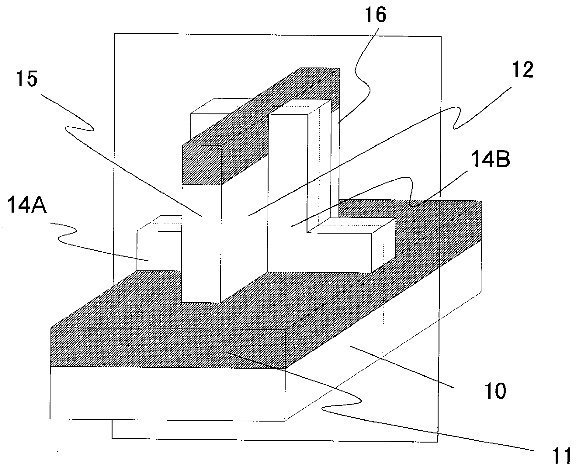
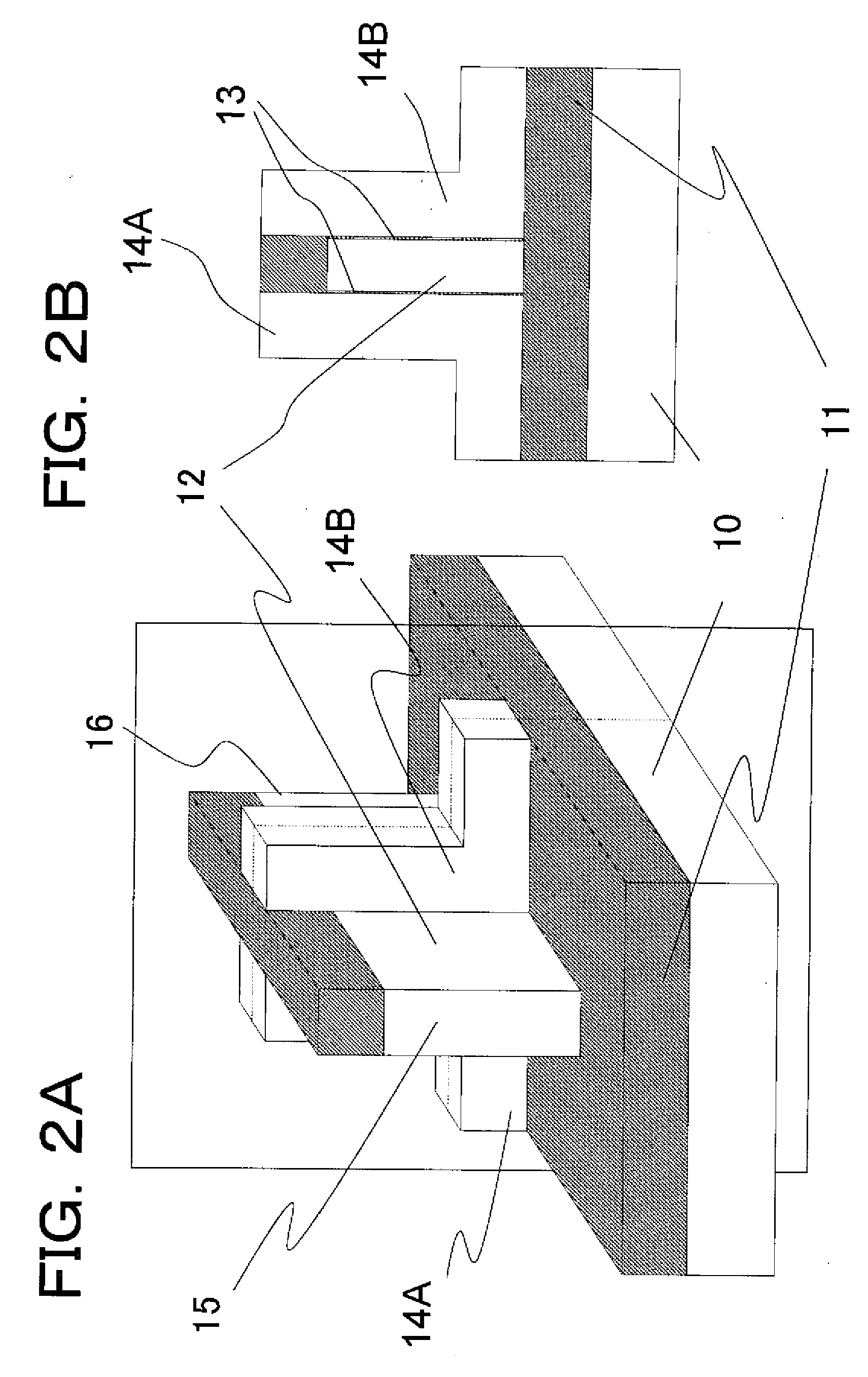
[0036] Referring to FIGS. 2 to 8, a memory cell array according to a first embodiment of the present invention is described below.

[0037]FIGS. 2A and 2B show a memory cell including one MOSFET (Metal Oxide Semiconductor Field Effect transistor) for use in a DRAM (Dynamic Random Access Memory) of the type called a 1T-DRAM. FIG. 2A is a perspective of the memory cell, and FIG. 2B is a cross-sectional view of the memory cell, taken along a plane shown in the perspective view of FIG. 2A. The memory cell shown in FIG. 2 is in accordance with the first embodiment of the invention. The memory cell shown in FIG. 2 is based on a memory cell using a fin-FET proposed in Japanese Patent Application No. 2004-141876 filed by the present applicant.

[0038] The fin-FET is a MOSFET formed in a 3-dimensional isolated region of a semiconductor formed on an SOI (Silicon On Insulator) substrate used as an insulating substrate. A source region is formed in a region including a first side surface of the 3-...

second embodiment

[0093] Referring to FIGS. 9 to 12, a memory cell array according to a second embodiment of the present invention is described below.

[0094] The memory cell array according to the second embodiment is composed of memory cells which are similar to those according to the first embodiment except that each back gate region, each source region, each front gate region, and each drain region are shaped by adjacent memory cells.

[0095]FIGS. 9A, 9B, 9C, 9D, and 9E show the memory cell array according to the second embodiment of the present invention.

[0096] In FIGS. 9A to 9E, reference numerals 70 denote SL lines, reference numeral 71 denotes a BG line, reference numerals 72 denote FG lines, reference numerals 73 denote BL lines, reference numerals 74 denote 3-dimensional isolated regions of silicon called fin regions in each of which a memory cell is formed, reference numeral 75 denotes a back gate region, reference numerals 76 denote front gate regions, reference numeral 77 denotes a contac...

third embodiment

[0132] Referring to FIG. 13, a memory cell array according to a third embodiment of the present invention is described below. The memory cell array according to the third embodiment is composed of memory cells which are similar to those according to the second embodiment except that fin regions in which memory cells are formed are connected in drain regions of memory cells adjacent in the row direction.

[0133]FIG. 13 shows a plan view of the memory cell array according to the third embodiment of the present invention. In FIG. 13, reference numerals 105 denote SL lines, reference numeral 106 denotes a BG line, reference numerals 107 denote FG lines, reference numerals 108 denote BL lines, reference numeral 109 denotes a 3-dimensional isolated region of silicon called a fin region in which a memory cell is formed, reference numeral 113 denotes a contact hole for contact with a corresponding back gate region of a memory cell (hereinafter such a contact hole will be referred to as a BG ...


PUM


Abstract

A memory cell array includes isolated semiconductor regions formed on a supporting insulating substrate, memory cells formed in the respective semiconductor regions, and insulating regions formed so as to insulate the memory cells. Each memory cell formed in a semiconductor region includes a source region, a drain region, a front gate region formed on a gate insulating film formed on one of side surfaces of the semiconductor region such that the source region and the drain region are separated from each other by the front gate region, and a back gate region formed on a gate insulating film formed on an opposite side surface of the semiconductor region such that the source region and the drain region are separated from each other by the back gate region. Each memory cell shares the back gate region with a memory cell adjacent in a row direction.

Description

BACKGROUND OF THE INVENTION [0001] 1. Field of the Invention [0002] The present invention relates to a memory cell array in which fin-FET memory cells of DRAM are arranged in the form of an array and which is advantageous for use as a memory device embedded in an LSI, a method of producing such a memory cell array, and a semiconductor device using such a memory cell array. More specifically, the present invention relates to a fin-FET memory cell array of DRAM, which can be disposed in a reduced area without causing a problem of multiple selection, a method of producing such a memory cell array, and a semiconductor circuit device using such a memory cell array. [0003] 2. Description of the Related Art [0004] State-of-the-art high-density LSIs include a huge number of logic circuits and an embedded memory. In such an LSI, an embedded memory part occupies a large area relative to the total chip area. In order to further increase the integration density of LSIs to meet requirements for ...

Claims


Application Information

Patent Timeline
IPC IPC(8): H01L27/12
CPCH01L21/845H01L27/108H01L27/10802H01L27/10826H01L29/785H01L27/1211H01L29/66795H01L29/7841H01L27/10879H01L29/6681H10B12/20H10B12/36H10B12/00H10B12/056H10B99/00
Inventor YOSHIDATANAKA, TETSUMIYASHITA, TOSHIHIKO
Owner FUJITSU LTD
Learn More