Semiconductor device

a technology of semiconductors and devices, applied in the direction of semiconductor devices, transistors, electrical apparatus, etc., can solve the problems of reducing the impurity concentration in the vicinity of the sti, affecting the accuracy of the microscopic region, so as to suppress the characteristic of the hump

Inactive Publication Date: 2007-12-06
PANASONIC CORP
View PDF5 Cites 8 Cited by
  • Summary
  • Abstract
  • Description
  • Claims
  • Application Information

AI Technical Summary

Benefits of technology

[0011]It is therefore an object of the present invention to provide a semiconductor device in which hump characteristics are suppressed and which can be fabricated in an easier manner than conventional semiconductor devices.

Problems solved by technology

However, in a semiconductor device fabricated using a STI device-isolation method, the transistor's threshold-voltage characteristics may degrade.
Impurities introduced into the channel region diffuse into the STI during an annealing process performed in the semiconductor device fabrication process, resulting in a decrease in impurity concentration in the vicinity of the STI.
It is very difficult to cover such a microscopic region with high accuracy.

Method used


Image

  • Semiconductor device
  • Semiconductor device
  • Semiconductor device

Examples


first embodiment

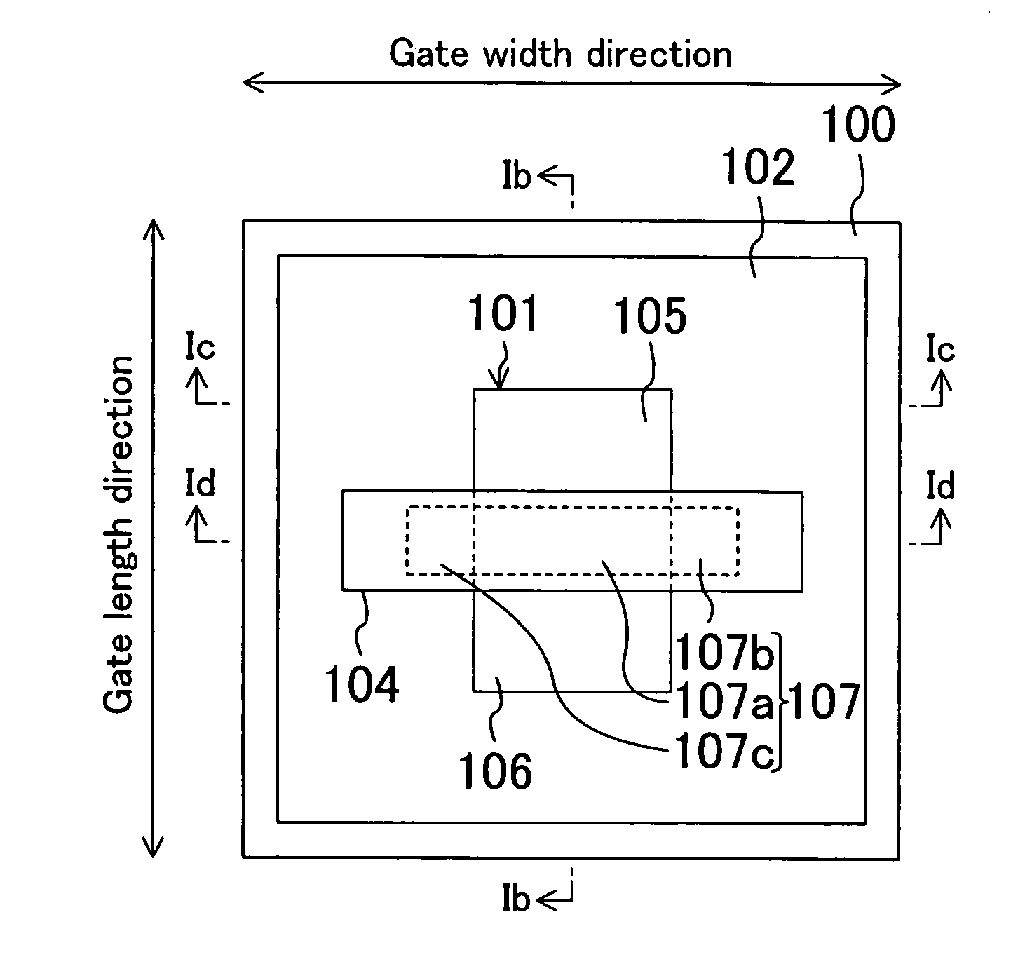
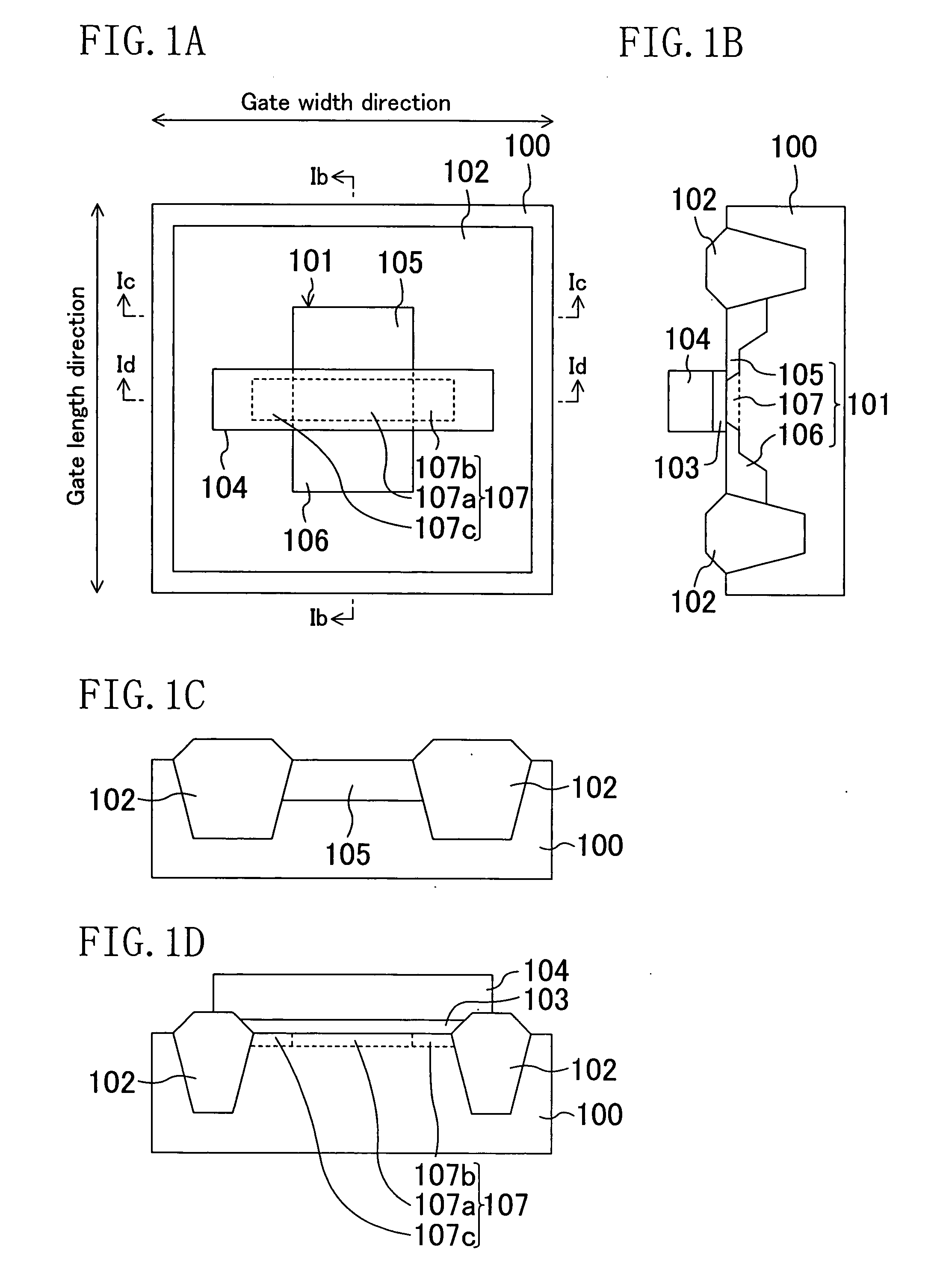
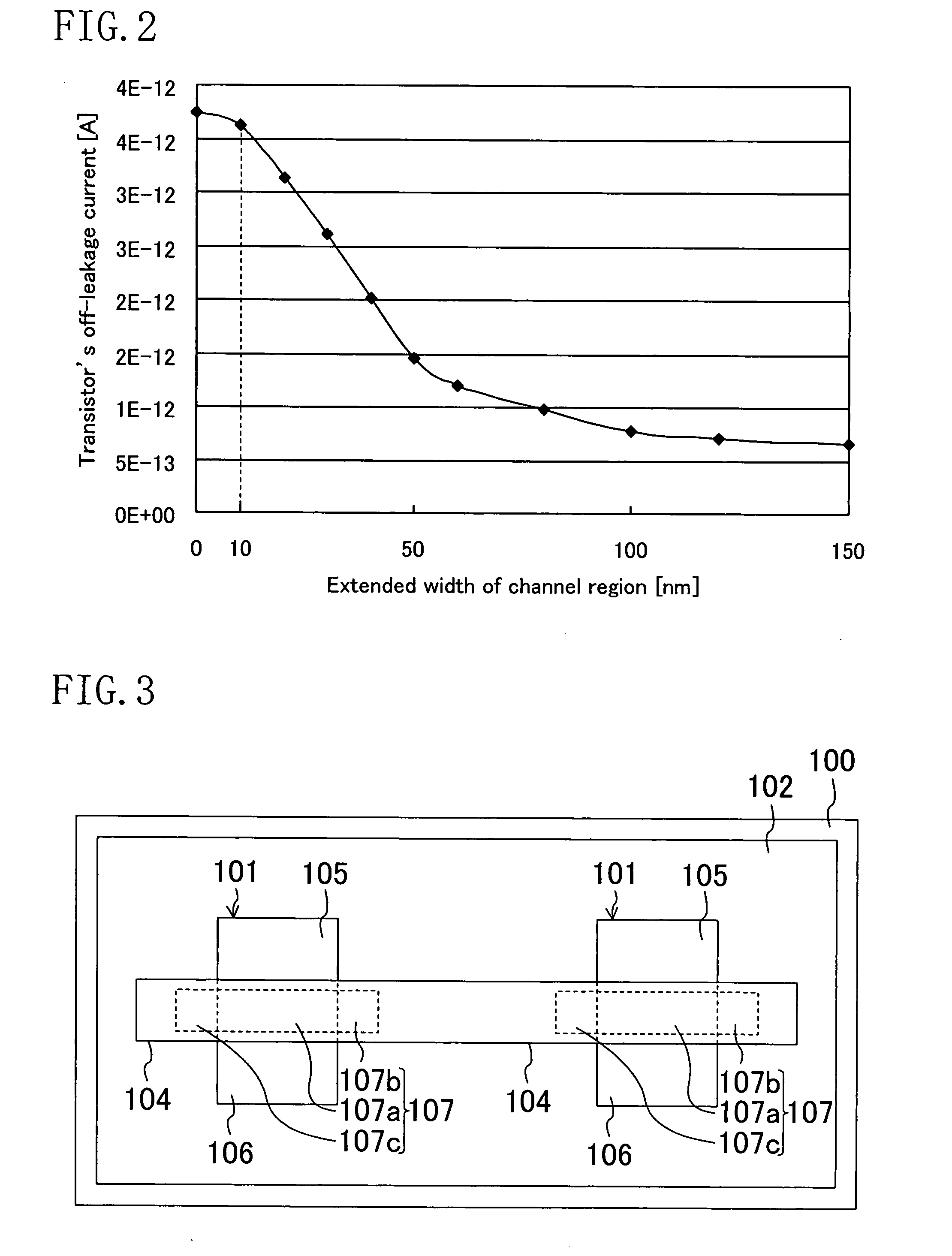
[0032]FIG. 1A is a plan view illustrating a semiconductor device according to a first embodiment of the present invention. FIGS. 1B, 1C, and 1D are cross-sectional views of the semiconductor device taken along the lines Ib-Ib, Ic-Ic, and Id-Id, respectively, in FIG. 1A.

[0033]The semiconductor device includes a semiconductor substrate 100, a device active portion 101, a device isolation portion 102, a gate insulating film 103, and a gate electrode 104.

[0034]The device active portion 101 is formed in the principal surface of the semiconductor substrate 100. The device isolation portion 102, which is a STI (shallow trench isolation), for example, is formed in the principal surface of the semiconductor substrate 100 so as to surround the periphery of the device active portion 101. The gate electrode 104 is stacked over the device active portion 101 with the gate insulating film 103 interposed therebetween.

[0035]The device active portion 101 includes a source region 105, a drain region 1...


PUM


Abstract

A semiconductor device includes: a semiconductor substrate; a device active portion formed in the semiconductor substrate; a device isolation portion formed in the semiconductor substrate so as to surround the periphery of the device active portion; an insulating film stacked on the device active portion; and a gate electrode stacked on the insulating film. The device active portion includes: a source region and a drain region located opposite each other in a gate length direction, and a channel region interposed between the source region and the drain region. The channel region includes: a central region connecting the source and drain regions and having an approximately rectangular shape, and a protruding region protruding from one side end of the central region in a gate width direction. The channel region is located inwardly of the gate electrode when viewed in the stacking direction.

Description

BACKGROUND OF THE INVENTION[0001]1. Field of the Invention[0002]The present invention relates to semiconductor devices, and more particularly relates to a semiconductor device including a device isolation portion formed using STI (shallow trench isolation).[0003]2. Description of the Related Art[0004]A semiconductor integrated circuit includes insulted-gate field-effect transistors (hereinafter referred to as “transistors”). In the semiconductor substrate, these transistors are electrically separated from each other by a device isolation portion. A method for forming such a device isolation portion is a device isolation method using STI (shallow trench isolation). A STI is formed by forming trenches in the semiconductor substrate and then filling the trenches with insulating material. STI, which allows the formation of a device isolation portion having a narrow isolation width, is a mainstream device-isolation method in recent microscaled fabrication processes.[0005]However, in a se...

Claims


Application Information

Patent Timeline
Patent Type & Authority Applications(United States)
IPC IPC(8): H01L29/00
CPCH01L29/6659H01L21/76224H01L29/78H01L29/1033H01L29/0692
Inventor IMADE, MASAHIRO
Owner PANASONIC CORP
Why Eureka
Try Eureka