Compound-Eye Imaging Device

Inactive Publication Date: 2007-12-13
FUNAI ELECTRIC CO LTD
View PDF5 Cites 14 Cited by
  • Summary
  • Abstract
  • Description
  • Claims
  • Application Information

AI Technical Summary

Benefits of technology

[0008] An object of the present invention is to provide a compound-eye imaging device which can prevent lights emitted from optical lenses from being reflected by an inner wall s

Problems solved by technology

In the conventional compound-eye imaging device 100, there is a problem in the quality of formed images.
Because of the existence of both the direct

Method used


Image

  • Compound-Eye Imaging Device
  • Compound-Eye Imaging Device
  • Compound-Eye Imaging Device

Examples


first embodiment

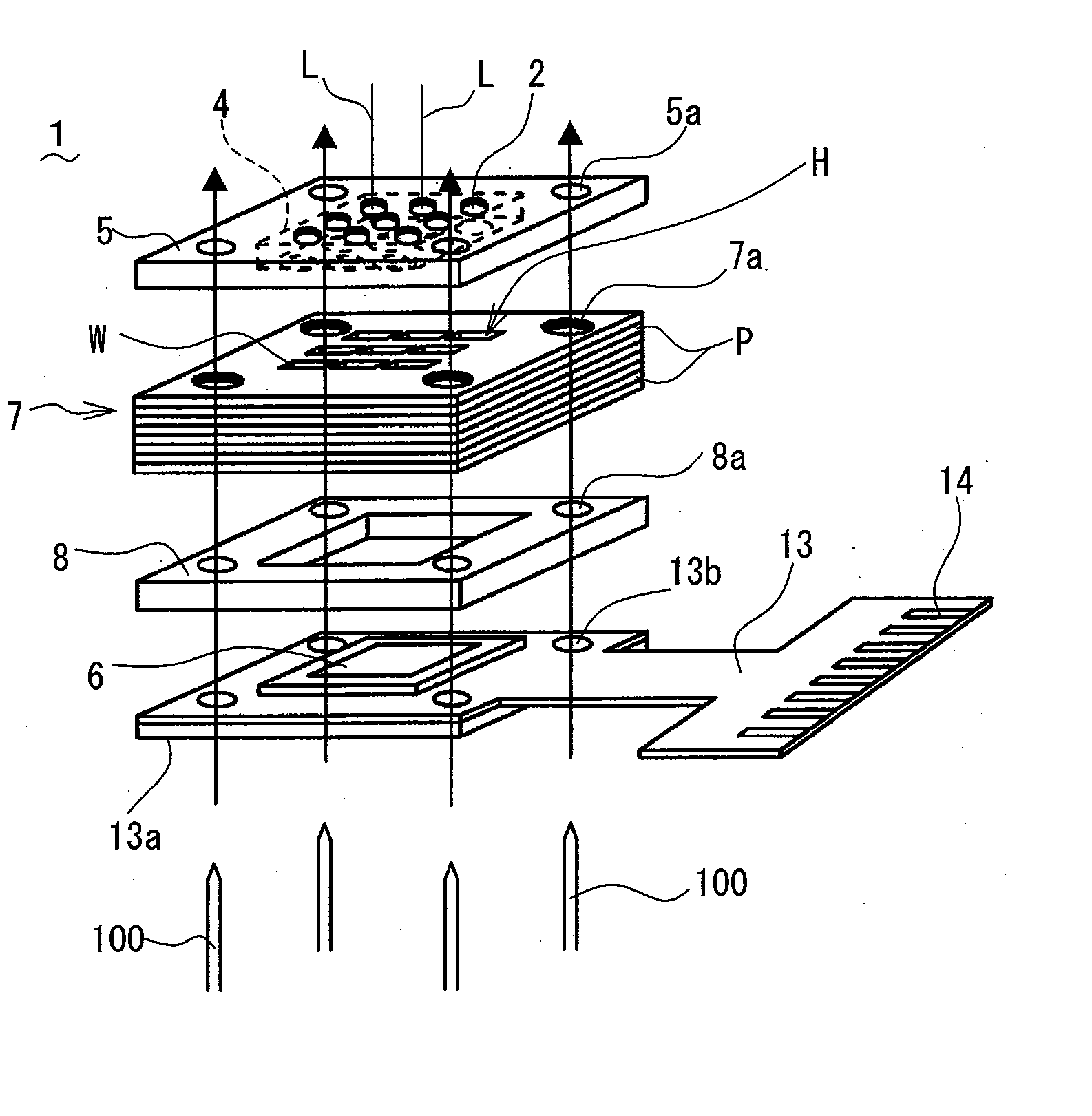
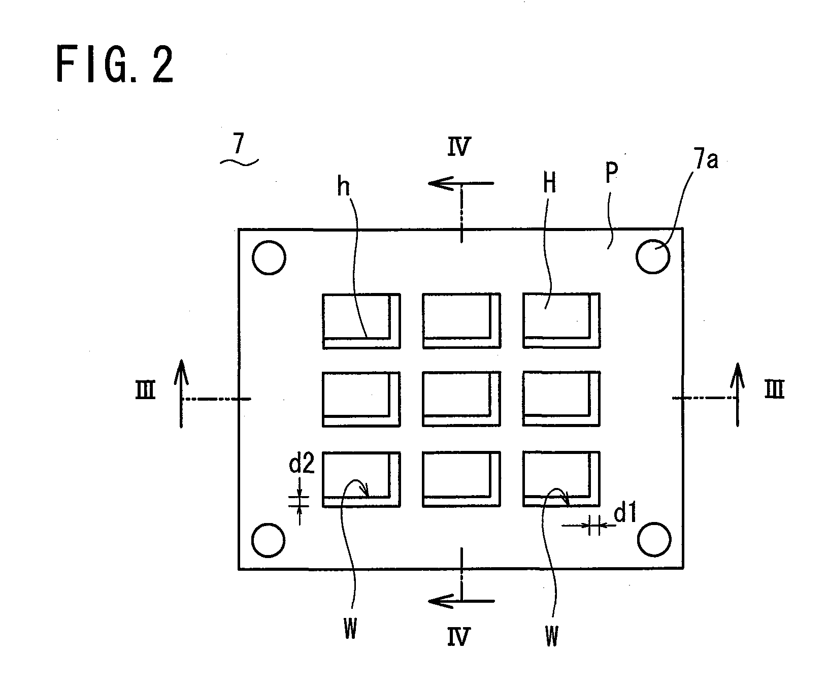
[0030] Referring to FIG. 1 to FIG. 5, a first embodiment of the present invention will be described. FIG. 1 is a schematic exploded perspective view of a compound-eye imaging device 1 according to the present embodiment when assembling the same in its entirety. FIG. 2 is a schematic plan view of a light shielding block 7. FIG. 3 and FIG. 4 are schematic vertical cross-sectional views of the compound-eye imaging device 1 along line III-III and line IV-IV of FIG. 2, respectively, showing, in addition to the light shielding block 7, a lens holder 5 and a photodetector array 6 in the compound-eye imaging device 1. As shown in FIG. 1, FIG. 3 and FIG. 4, the compound-eye imaging device 1 comprises: an optical lens array 4 having 9 (nine) optical lenses 2 which have optical axes L parallel to each other, and which are arranged in a matrix of three rows and three columns and integrally formed as single convex lenses on a lower surface of one transparent substrate 3; and a lens holder 5 for ...

second embodiment

[0046] Referring now to FIG. 6 to FIG. 8, a second embodiment of the present invention will be described. FIG. 6 is a schematic plan view of a light shielding block 7 used in a compound-eye imaging device 1 according to the second embodiment. FIG. 7A and FIG. 7B are schematic plan views of a first unit plate P1 and a second unit plate P2, respectively, to form the light shielding block 7. On the other hand, FIG. 8 is a schematic vertical cross-sectional view of the compound-eye imaging device 1 along line VIII-VIII of FIG. 6, showing, in addition to the light shielding block 7, a lens holder 5 and a photodetector array 6 in the compound-eye imaging device 1. The compound-eye imaging device 1 of the second embodiment is similar to that of the first embodiment, except that the light shielding block 7 here is formed of two kinds of unit plates P1, P2 stacked on each other which are different from each other in shape. Thus, except for the unit plates, the other elements of the compound-...

third embodiment

[0050] Referring now to FIG. 9, a third embodiment of the present invention will be described. FIG. 9 is a schematic vertical cross-sectional view, corresponding to the vertical cross-sectional view of FIG. 3, FIG. 4 and FIG. 8, of a compound-eye imaging device 1 according to the third embodiment. A feature of the compound-eye imaging device 1 of the present embodiment is that, as shown in FIG. 9, each of the unit plates P has a tapered surface on an inner wall surface Wa in each of the light-passing windows W therein so as to form an irregular or uneven inner wall surface Ha, which serves as a light scattering surface, in each of the light-passing holes H of the light shielding block 7. Except for this difference in the way of the formation of the inner wall surface Ha, the compound-eye imaging device 1 of the present embodiment is similar to that of the first or the second embodiment. Thus, the other elements of the compound-eye imaging device 1 of the present embodiment are desig...


PUM


Abstract

A compound-eye imaging device comprises: an optical lens array with integrated optical lenses; a stop member; a photodetector array for imaging multiple images formed by the optical lenses; and a light shielding block for partitioning a space between the two arrays into a matrix of spaces, with light-passing holes, so as to prevent lights emitted from the optical lenses from interfering each other. The light shielding block is formed of unit plates in a stack, each having light-passing windows. Each light-passing window has blackened surface. The unit plates in the stack are alternately reversed upside down and left-right so as to allow the horizontal positions of the light-passing windows for forming each light-passing hole through the unit plates in the stack to be alternately offset in depth direction of the hole, thereby forming an irregular inner wall surface which serves as a light scattering surface to prevent e.g. ghost.

Description

BACKGROUND OF THE INVENTION [0001] 1. Field of the Invention [0002] The present invention relates to a compound-eye imaging device having an optical imaging system which is formed of multiple micro optical systems so as to reduce the focal length, making it possible to reduce the thickness of the compound-eye imaging device. [0003] 2. Description of the Related Art [0004] There has been developed a compound-eye imaging device as a thin camera module to be installed in a cellular phone, a personal computer, or the like. The compound-eye imaging device is mainly composed of: an optical lens array with multiple integrated optical lenses; a photodetector array for imaging multiple images formed by the respective optical lenses of the optical lens array; and an image reconstructing circuit for reconstructing the multiple images, imaged by the photodetector array, into one image by using parallax information between the multiple images. [0005] It is known to form an image input unit by pl...

Claims


Application Information

Patent Timeline
IPC IPC(8): H01L27/00G02B7/02H04N5/225H04N5/335H04N5/345H04N5/359
CPCG02B3/0006G02B3/0056G02B3/0075H04N5/2257H01L27/14627H04N5/2253H04N5/2254H01L27/14623H04N23/54H04N23/57
Inventor TOYODA, TAKASHINAKAO, YOSHIZUMIMASAKI, YASUO
Owner FUNAI ELECTRIC CO LTD
Why Eureka
Try Eureka