Semiconductor device

a technology of semiconductor elements and semiconductor components, applied in the field of semiconductor devices, can solve the problems of difficult to constitute a power source for the digital semiconductor element, difficult to analog semiconductor elements, and low noise band required by analog rf signals

Inactive Publication Date: 2007-12-20
RENESAS ELECTRONICS CORP
View PDF9 Cites 63 Cited by
  • Summary
  • Abstract
  • Description
  • Claims
  • Application Information

AI Technical Summary

Benefits of technology

[0010] Another object of the present invention is to provide a technique capable of securing quality of signals in the semiconductor device and achieving stabilization of a power source.
[0017] Since the power layer for the analog element of a printed board is connected to one end of the EBG layer, the power layer for a digital element is connected to the other end, the ground connecting terminals for the respective elements are connected to a common ground layer, and a ground layer for separating the power layer for the analog element and the EBG layer from each other is arranged therebetween, high-density mounting can be achieved while reducing interference of power source noise to the analog semiconductor element.

Problems solved by technology

However, a noise band required by an analog RF signal is considerably low (for example, −120 dBm in GPS).
It is a problem that, because of transmission / reception of the analog RF signal and interference of noise generated from the digital semiconductor element, it is difficult for the analog semiconductor element and the digital semiconductor element to share a power source and mount the analog semiconductor element and the digital semiconductor element so as to be close to each other.
That is, since interference of power source noise from the digital semiconductor element to the analog semiconductor element exists, it is difficult to constitute a power source for the digital semiconductor element and for the analog semiconductor element as a common power source and realize proximity mounting for high-density mounting.

Method used


Image

  • Semiconductor device
  • Semiconductor device
  • Semiconductor device

Examples


first embodiment

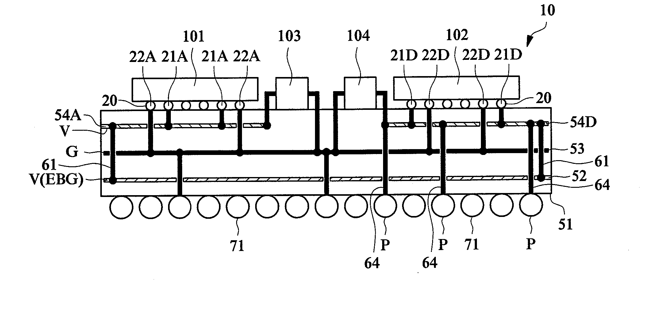
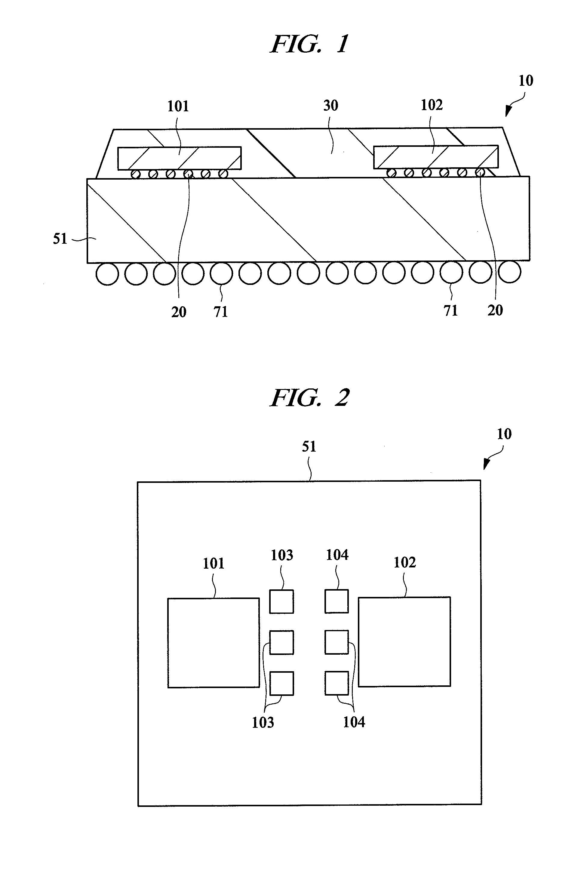
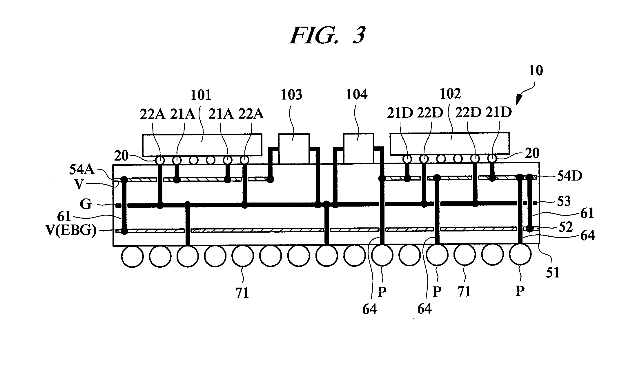
[0060]FIG. 1 is a cross-sectional diagram showing one example of a structure of a semiconductor device according to a first embodiment of the present invention, FIG. 2 is a plan diagram showing one example of a mounting layout of parts in the semiconductor device shown in FIG. 1, and FIG. 3 is a structural diagram showing one example of routing of inner wire over a package board of the semiconductor device shown in FIG. 1. And, FIG. 4 is a plan diagram showing one example of a structure of a power layer for an analog element and a power layer for a digital element provided over the package board of the semiconductor device shown in FIG. 1, FIG. 5 is a plan diagram showing one example of a structure of a ground layer provided over the package board of the semiconductor device shown in FIG. 1, FIG. 6 is a plan diagram showing one example of a structure of an EBG layer provided over the package board of the semiconductor device shown in FIG. 1, and FIG. 7 is a back diagram showing one ...

second embodiment

[0092]FIG. 12 is a structural diagram showing one example of routing of inner wire in a package board of a semiconductor device according to a second embodiment of the present invention.

[0093] In a SIP (semiconductor device) 10 according to the second embodiment, the power layer for digital 54D is arranged on a side near a back face of the package board 51. That is, the power layer for digital 54D is disposed between the EBG layer 52 and the solder balls 71. Thereby, in a layer including a wiring layer of the power layer for digital 54D, wires for digital signal can be formed in a region corresponding to a portion just below the power layer for analog 54A, so that a wire use rate can be improved.

[0094] Note that, since the power layer for digital 54D is arranged on a side near the back face of the package board 51, the power layer for digital 54D can be connected to the solder balls 71 with a shortest route by shortening the digital power source connection viaholes 64. Thereby, co...

third embodiment

[0097]FIG. 13 is a structural diagram showing one example of routing of inner wire in a package board of a semiconductor device according to a third embodiment of the present invention.

[0098]FIG. 13 is a diagram showing respective signal wires of the analog chip 101 and the digital chip 102 in the SIP (semiconductor device) 10 according to the third embodiment. Signal area for analog (signal area for analog element) 55A is wired adjacent to the power layer for analog 54A or the ground layer 53 to connect the analog chip 101 and the solder balls 71 to each other. For example, the signal area for analog 55A is disposed between the analog chip 101 and the power layer for analog 54A along the power layer for analog 54A and connects signal connection terminals for analog 23A that are signal connection terminals for the analog chip 101 and the solder balls 71 for analog signal.

[0099] By disposing the signal area for analog 55A adjacent to the power layer for analog 54A or the ground lay...


PUM


Abstract

The present invention realizes high density mounting along with achieving power source sharing by a digital semiconductor element and an analog semiconductor element in a semiconductor device. An power layer for analog is connected to one end of an EBG layer, a power layer for digital is connected to the other end of the EBG layer, ground terminals for the respective elements are connected to a common ground layer, and a ground layer for separating the power layer for analog and the EBG layer from each other is disposed between the power layer for analog and the EBG layer. Thereby, high density mounting is achieved along with reducing interference of power source to an analog chip.

Description

CROSS-REFERENCE TO RELATED APPLICATION [0001] The present application claims priority from Japanese Patent Application No. JP 2006-155136 filed on Jun. 2, 2006, the content of which is hereby incorporated by reference into this application. TECHNICAL FIELD OF THE INVENTION [0002] Present invention relates to a semiconductor device, and in particular to an effective technique in application to a semiconductor device having an analog semiconductor element and a digital semiconductor element. BACKGROUND OF THE INVENTION [0003] In a portable electronic device such as GPS (Global Positioning System) or wireless LAN (Local Area Network), it is required to combine a wireless technique and a high-density mounting technique. And therefore, a demand for mounting an analog semiconductor element and a digital semiconductor element so as to be close to each other or on one package is increasing. A technique for mounting an analog semiconductor element and a digital semiconductor element on the s...

Claims


Application Information

Patent Timeline
Patent Type & Authority Applications(United States)
IPC IPC(8): H05K1/00
CPCH01L23/66H01L25/0655H01L2924/30107H01L2225/06558H01L2924/19105H01L25/0657H01L25/16H01L25/18H01L2224/16225H01L2224/48091H01L2224/48227H01L2225/0651H01L2225/06517H01L2225/06541H01L2924/15311H01L2924/3011H01L2924/3025H05K1/0231H05K1/0236H05K1/0237H05K1/141H05K2201/093H05K2201/09309H05K2201/09663H05K2201/09681H05K2201/09727H05K2201/09972H05K2201/10734H01L24/48H01L2224/16145H01L2924/15192H01L2924/00014H01L2924/00H01L2924/14H01L2224/45099H01L2224/45015H01L2924/207H01L23/12
Inventor OSAKA, HIDEKIUEMATSU, YUTAKASUZUKI, EIICHI
Owner RENESAS ELECTRONICS CORP
Why Eureka
Try Eureka