Increased open-circuit-voltage organic photosensitive devices
a photosensitive device and open-circuit voltage technology, applied in the direction of solid-state devices, semiconductor devices, thermoelectric devices, etc., can solve the problems of low power conversion efficiency and sub>p/sub>) of organic photosensitive devices, and achieve the effect of low fcs
- Summary
- Abstract
- Description
- Claims
- Application Information
AI Technical Summary
Benefits of technology
Problems solved by technology
Method used
Image
Examples
Embodiment Construction
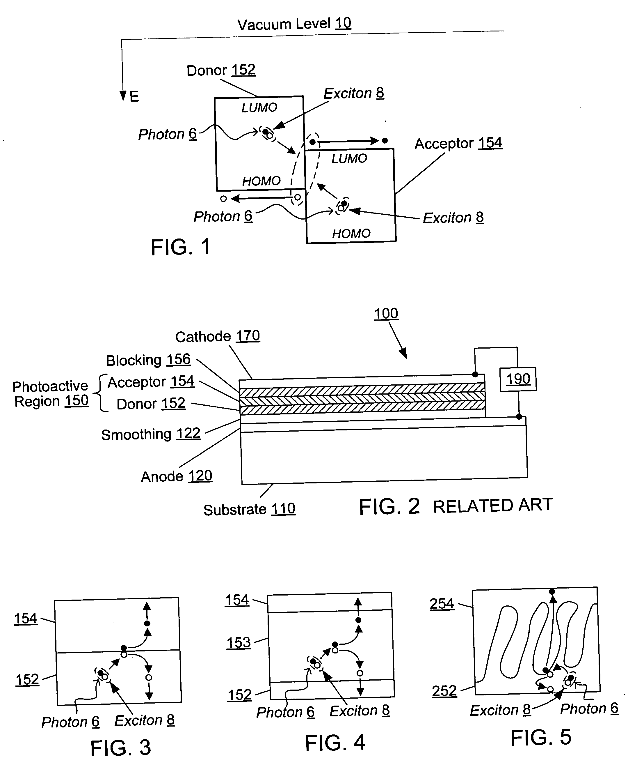
[0046] An organic photosensitive device comprises at least one photoactive region in which light is absorbed to form an exciton, which may subsequently dissociate into an electron and a hole. FIG. 2 shows an example of an organic photosensitive optoelectronic device 100 in which the photoactive region 150 comprises a donor-acceptor heterojunction. The “photoactive region” is a portion of a photosensitive device that absorbs electromagnetic radiation to generate excitons that may dissociate in order to generate an electrical current. Device 100 comprises an anode 120, an anode smoothing layer 122, a donor 152, an acceptor 154, an exciton blocking layer (“EBL”) 156, and a cathode 170, over a substrate 110.
[0047] Examples of EBL 156 are described in U.S. Pat. No. 6,451,415 to Forrest et al., which is incorporated herein by reference for its disclosure related to EBLs. Additional background explanation of EBLs may also be found in Peumans et al., “Efficient photon harvesting at high op...
PUM
 Abstract
Description
Claims
Application Information


