Die package and probe card structures and fabrication methods

a probe card and probe technology, applied in the direction of solid-state devices, basic electric elements, instruments, etc., can solve the problems of lead frame-based packaging, difficult, if not impossible in some circumstances, and the inner end of the lead finger of the lead frame in close proximity to the bond pad, and risking the potential breakage of the wire bond or shorting between adjacent wire bonds

Active Publication Date: 2007-12-27
MICRON TECH INC
View PDF2 Cites 84 Cited by
  • Summary
  • Abstract
  • Description
  • Claims
  • Application Information

AI Technical Summary

Problems solved by technology

As a consequence, it becomes more difficult to employ lead frame-based packaging techniques using, for example, wire bonds to connect bond pads of a die to lead fingers of a lead frame due to diminishing size of bond pads as well as decreasing pitch (spacing) between adjacent bond pads, rendering it difficult, if not impossible in some circumstances, to place inner ends of lead fingers of a lead frame in close proximity to bond pads to which they are to be wire bonded.
Further, when bond pads are arranged along a central axis of a semiconductor die, such as is conventional in so-called “leads over chip,” or “LOC” packages, one may be faced with a choice between elongating and overcrowding lead fingers to place them in close proximity to the bond pads, or forming overly long wire bonds between the bond pads and remotely placed inner ends of lead fingers and risking potential breakage of the wire bonds or shorting between adjacent wire bonds when the package is being transfer-molded in an encapsulant by so-called “wire bond sweep” initiated by the flow front of the molten encapsulant moving over the active surface of the semiconductor die.
In addition, most conventional, lead frame-based packages do not facilitate high device density in conjunction with high multi-die device yields in terms of utilizing available “real estate” on a printed circuit board or other higher-level packaging.
It has also been recognized by those of ordinary skill in the art that it is desirable to probe test multiple semiconductor dice simultaneously, and that some dice employ bond pad configurations which render it difficult to fabricate probe cards suitable for probe testing a plurality of such dice without using a substrate including multiple layers of conductive traces.
Further, in order to accommodate some bond pad configurations, it may be necessary to provide fairly long conductive paths from the location of a given interior contact to the periphery of the probe card substrate, inducing excessive capacitance, particularly if the paths comprise thin-film, planar metal traces.

Method used


Image

  • Die package and probe card structures and fabrication methods
  • Die package and probe card structures and fabrication methods
  • Die package and probe card structures and fabrication methods

Examples


Embodiment Construction

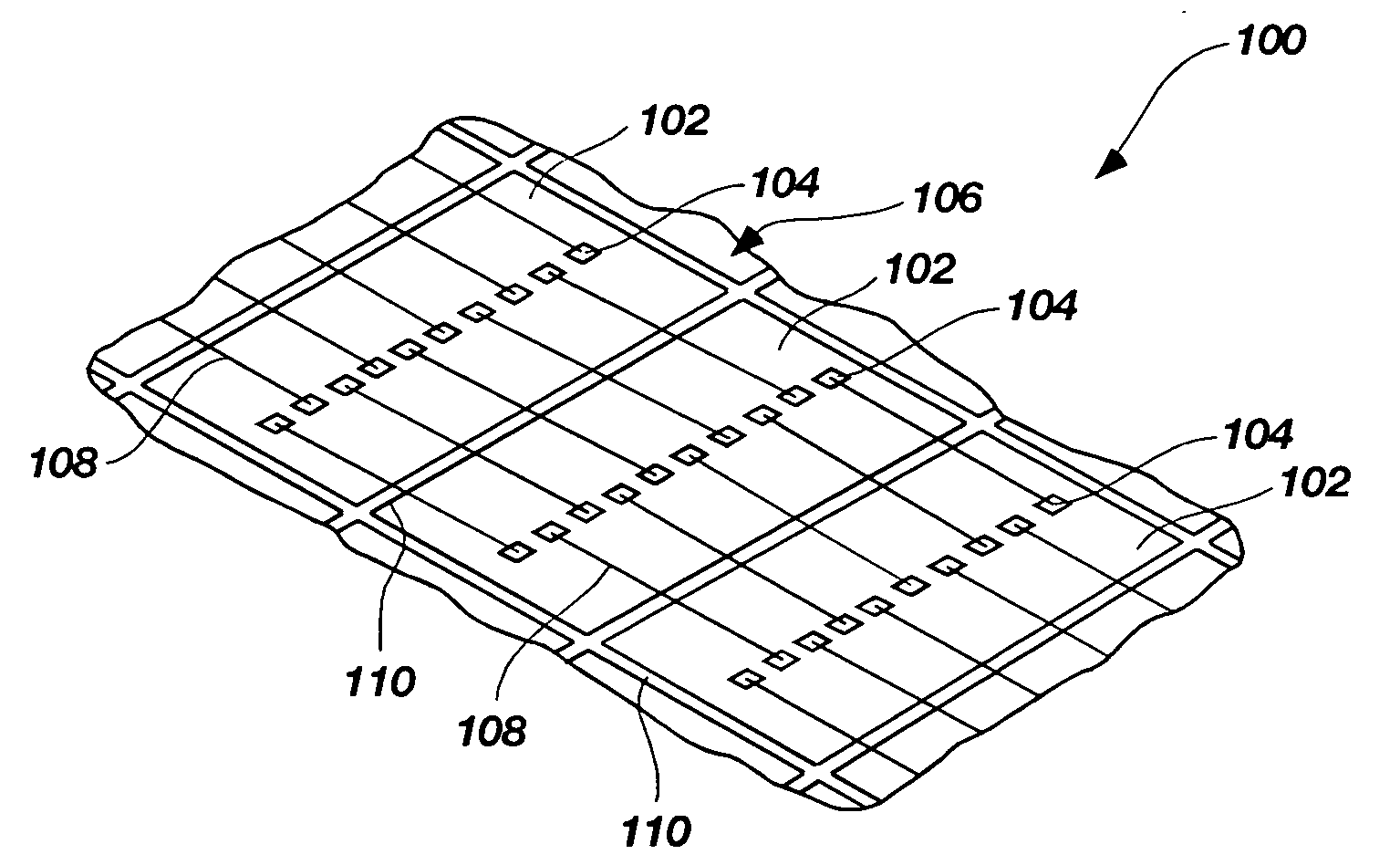
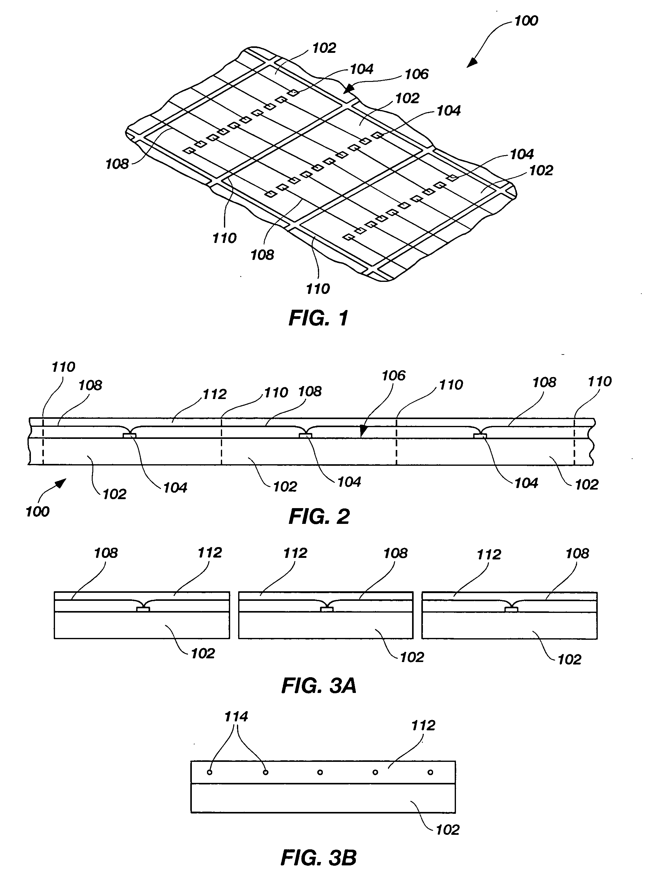
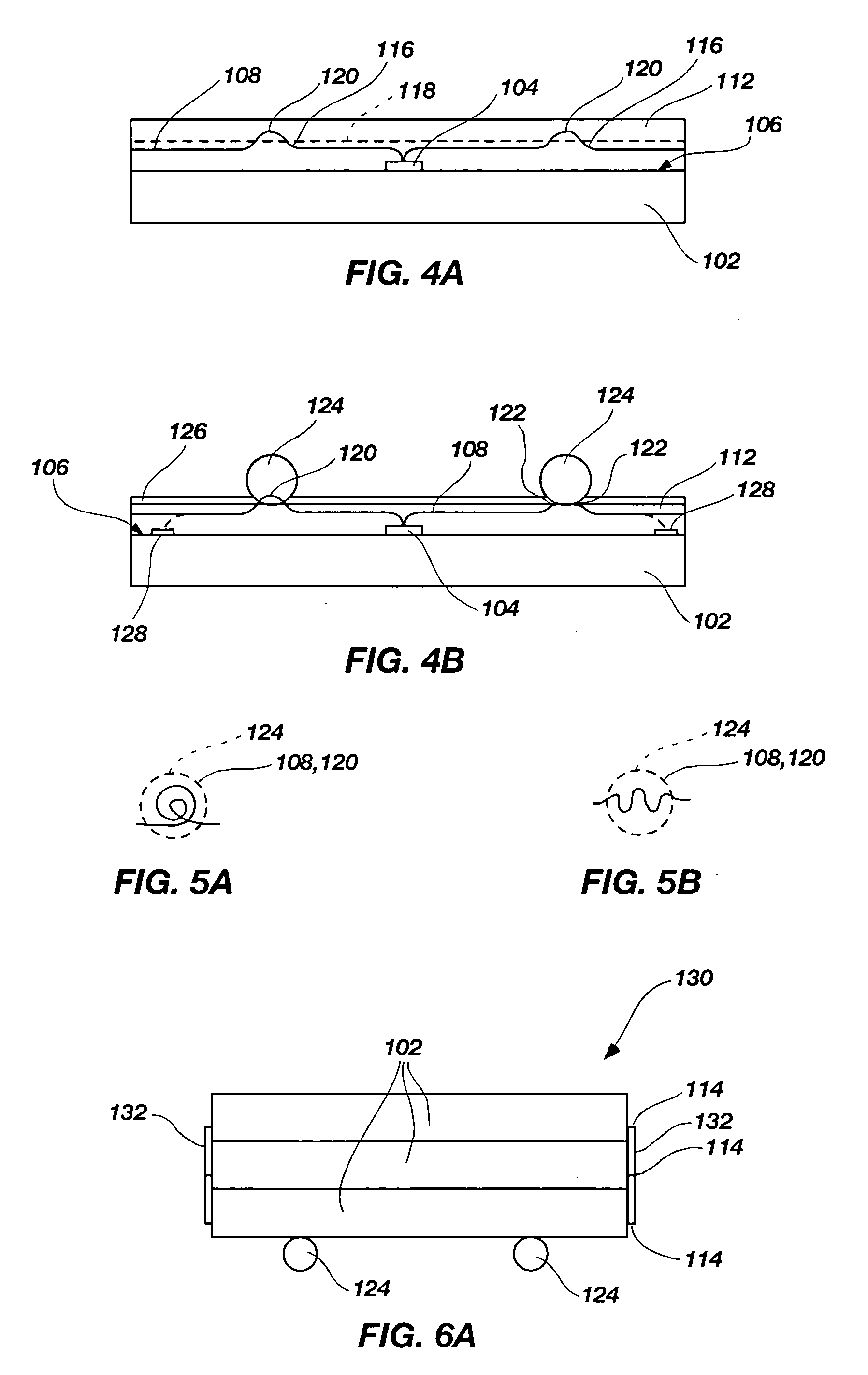
[0035]The present invention, in several embodiments, comprises single die and multi-die semiconductor device packages as well as methods of fabricating such packages and subcomponents thereof. The present invention also comprises probe cards configured for simultaneous wafer-level testing of multiple dice, and methods of fabrication thereof.

[0036]In one embodiment, the present invention comprises a method of forming individual semiconductor die assemblies which may be configured for use individually or stacked to form a multi-die package, in either case being provided with discrete conductive elements protruding transversely from a major surface thereof for use in connecting the package to higher-level packaging such as a printed circuit board.

[0037]Semiconductor dice in wafer or other bulk substrate form (each of which may be termed a “wafer” herein for the sake of convenience) may each be provided with one or more central rows of bond pads proximate a central longitudinal axis the...


PUM


Abstract

A semiconductor die has conductors encapsulated in a dielectric material disposed on the active surface extending across the active surface from bond pads to one or more peripheral edges where the conductor ends are disposed at a side surface of the dielectric material. Stacks of such semiconductor dice, wherein one of the dice is configured with discrete conductive elements projecting from the active surface, and the exposed ends of the dice in the stack are connected with vertical interconnects. A probe card is disclosed having bond wires extending from more central contacts between more peripheral contacts to the edge of the probe card. A probe card having an upper layer bearing contacts and at least one window therethrough, a lower layer bearing conductive traces with ends exposed through the at least one window, and conductors extending from at least some of the contacts to conductive trace ends is also provided. Methods of making the foregoing structures are disclosed.

Description

BACKGROUND OF THE INVENTION[0001]1. Field of the Invention[0002]The present invention relates generally to packaging of semiconductor devices and, more particularly, to single die and multi-die semiconductor device packages as well as to methods of fabricating such packages and subcomponents thereof. The present invention is also directed to methods of fabricating probe cards and resulting structures.[0003]2. Discussion of Related Art[0004]Semiconductor dice are becoming ever-smaller in dimension, both from advances in fabrication technology and as so-called “shrinks” of initial semiconductor die designs are developed to increase the number of dice which may be fabricated on a wafer or other bulk semiconductor substrate. As a consequence, it becomes more difficult to employ lead frame-based packaging techniques using, for example, wire bonds to connect bond pads of a die to lead fingers of a lead frame due to diminishing size of bond pads as well as decreasing pitch (spacing) betwee...

Claims


Application Information

Patent Timeline
IPC IPC(8): H01L23/52
CPCG01R1/07314G01R3/00H01L24/13H01L2924/01033H01L2924/01006H01L2924/00014H01L2924/30107H01L2924/30105H01L2924/20752H01L2924/09701H01L2924/014H01L2924/01082H01L2924/01079H01L2924/01078H01L2924/01049H01L2924/01031H01L2924/01029H01L23/4828H01L24/10H01L24/45H01L24/48H01L24/50H01L24/85H01L25/0657H01L2224/13099H01L2224/45015H01L2224/45124H01L2224/45144H01L2224/45147H01L2224/48091H01L2224/4813H01L2224/484H01L2224/48599H01L2224/48699H01L2224/48799H01L2224/4899H01L2224/85H01L2225/06551H01L2225/06596H01L2924/01005H01L2924/01013H01L2924/01014H01L2924/01015H01L2924/01027H01L2924/01028H01L2224/78H01L2924/00H01L2224/85203H01L2224/85207H01L2224/13H01L2224/05554H01L2224/05644H01L24/86H01L2224/45014B33Y80/00H01L24/05H01L2224/023H01L2924/206H01L2924/0001
Inventor HEMBREE, DAVID R.
Owner MICRON TECH INC
Why Eureka
Try Eureka