Multi-bit high-density memory device and architecture and method of fabricating multi-bit high-density memory devices

a memory device and high-density technology, applied in the field of multi-bit high-density memory devices and architecture, can solve problems such as yield loss and imperfect connections

Active Publication Date: 2008-01-03
AURIGA INNOVATIONS INC
View PDF9 Cites 90 Cited by
  • Summary
  • Abstract
  • Description
  • Claims
  • Application Information

AI Technical Summary

Benefits of technology

[0009]A seventh aspect of the present invention is the first aspect, wherein a pitch of the nano-fins of the array of nano-fins in a second direction perpendicular to the first direction is less than a smallest pitch lithographically definable by a photolithographic system used to define each the at least two gates.
[0010]An eighth aspect of the present invention is the first aspect, wherein a width of the nano-fins of the array of nano-fins in a second direction perpendicular to the first direction is less than about 50 nm.
[0011]A ninth aspect of the present invention is the first aspect, wherein a width, in a second direction, of gates of the first and second set of gates located between adjacent nano-fins of a same group of nano-fins is less than about 50 nm and a width, in the second direction, of gates of the first and second sets of gates located between nano-fins of adjacent groups of nano-fins is equal to or greater than about 180 nm, the second direction perpendicular to the first direction.

Problems solved by technology

However, there is a “pattern-mismatch” when normal photolithographic groundrule and sub-photolithographic groundrule structures are used in the same structure.
“Pattern-mismatch” can cause yield loss and imperfect connections.

Method used


Image

  • Multi-bit high-density memory device and architecture and method of fabricating multi-bit high-density memory devices
  • Multi-bit high-density memory device and architecture and method of fabricating multi-bit high-density memory devices
  • Multi-bit high-density memory device and architecture and method of fabricating multi-bit high-density memory devices

Examples


Embodiment Construction

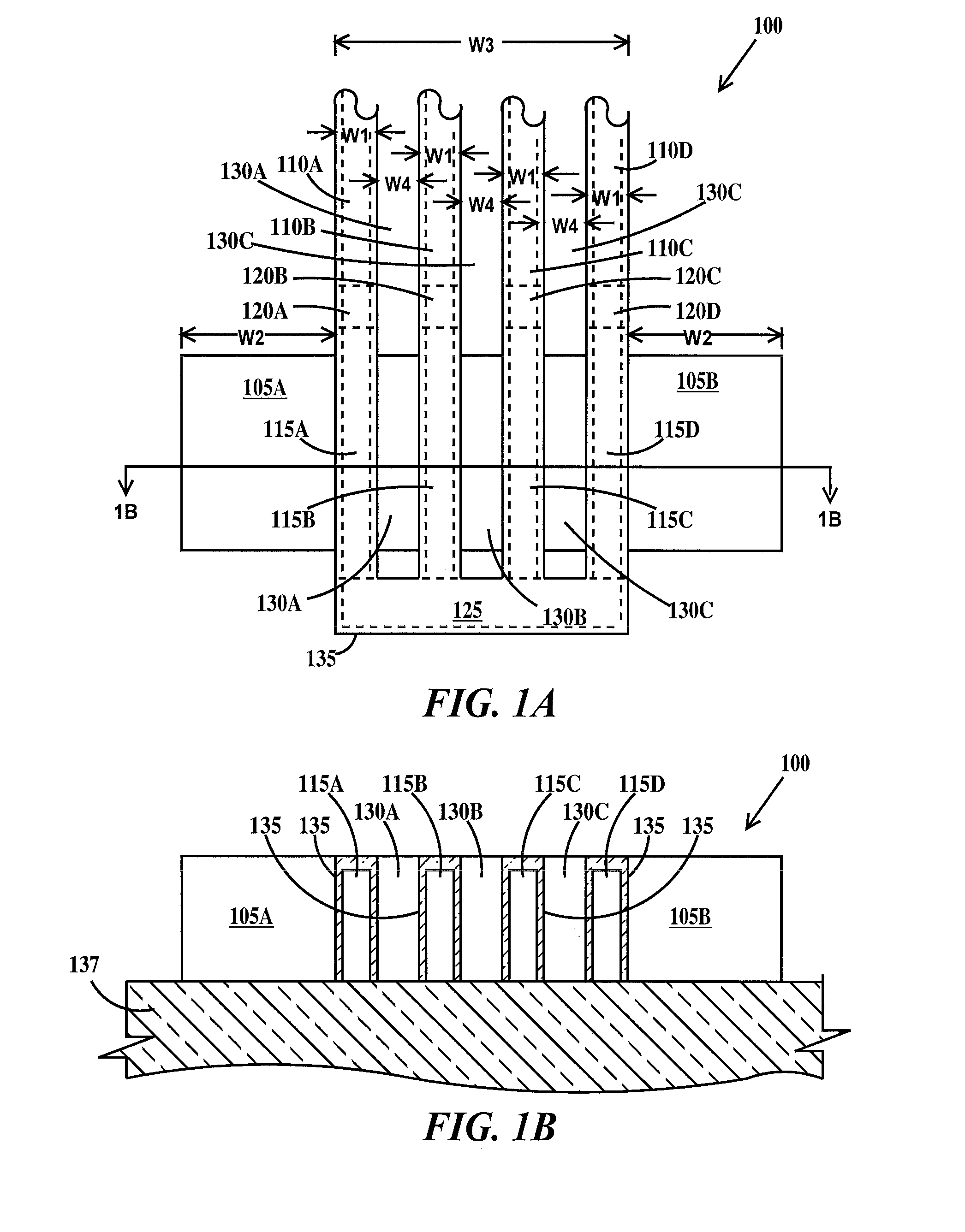
[0024]FIG. 1A is a top view and FIG. 1B is a cross-sectional view through line 1B-1B of FIG. 1A of a micro-to-nano address block (MNAB) illustrating the principles of operation of the MNAB. MNABs provide selection of the individual nano-fins of a nano-fin array. In FIGS. 1A and 1B, a MNAB 100 includes first and second polysilicon control gates 105A and 105B and single-crystal silicon nano-fins 110A, 110B, 110C and 110D. Nano-fins 110A, 110B, 110C and 110D include respective channel regions 115A, 115B, 115C and 115D and drain (or source) regions 120A, 120B, 120C and 120D and a common source (or drain) region 125. Channel regions 115A and 115B are separated by an electrically floating doped-polysilicon region 130A. Channel regions 115B and 115C are separated by an electrically floating doped-polysilicon region 130B. Channel regions 115C and 115D are separated by an electrically floating doped-polysilicon region 130C. Nano-fins 110A, 110B, 110C and 110D and first and second gates 105A ...


PUM


Abstract

A structure, memory devices using the structure, and methods of fabricating the structure. The structure includes: an array of nano-fins, each nano-fin comprising an elongated block of semiconductor material extending axially along a first direction, the nano-fins arranged in groups of at least two nano-fins each, wherein ends of nano-fins of each adjacent group of nano-fins are staggered with respect to each other on both a first and a second side of the array; wherein nano-fins of each group of nano-fins are electrically connected to a common contact that is specific to each group of nano-fins such that the common contacts comprise a first common contact on the first side of the array and a second common contact on the second side of the array; and wherein each group of nano-fins has at least two gates that electrically control the conductance of nano-fins of the each group of nano-fins.

Description

FIELD OF THE INVENTION[0001]The present invention relates to the field of semiconductor devices; more specifically, it relates to a multi-bit high-density memory device and architecture and methods of fabricating multi-bit high-density memory devices.BACKGROUND OF THE INVENTION[0002]In an effort to drastically increase the density of memory devices that are fabricated with conventional semiconductor processes and are compatible with conventional complimentary metal oxide silicon (CMOS) technology, efforts have been directed to devices that combine normal photolithographic groundrule and sub-photolithographic groundrule dimensions. However, there is a “pattern-mismatch” when normal photolithographic groundrule and sub-photolithographic groundrule structures are used in the same structure. “Pattern-mismatch” can cause yield loss and imperfect connections. Therefore, there is a need for an interface device, memory device, memory device architecture and method of fabricating memory devi...

Claims


Application Information

Patent Timeline
Patent Type & Authority Applications(United States)
IPC IPC(8): H01L27/10H01L29/74
CPCB82Y10/00H01L27/0207H01L27/115H01L29/785H01L29/0673H01L29/42336H01L29/0665Y10S438/947Y10S977/888Y10S977/936H10B69/00
Inventor GOPALAKRISHNAN, KAILASHSHENPY, ROHIT SUDHIR
Owner AURIGA INNOVATIONS INC
Why Eureka
Try Eureka