Reference voltage generation circuit

a reference voltage and circuit technology, applied in the direction of electric variable regulation, process and machine control, instruments, etc., can solve the problems of large power consumption and substantial fluctuations in output voltage vref, and achieve the effect of large power consumption

Active Publication Date: 2008-01-10
SOCIONEXT INC
View PDF3 Cites 25 Cited by
  • Summary
  • Abstract
  • Description
  • Claims
  • Application Information

AI Technical Summary

Benefits of technology

[0009]However, in the reference voltage generation circuit shown in FIG. 5 of Patent Document 1, a current flows not only through the first and second current paths but also through the third current path including the resistive element R2 and the diode D1, thus resulting in a large power consumption.

Problems solved by technology

However, in the reference voltage generation circuit shown in FIG. 5 of Patent Document 1, a current flows not only through the first and second current paths but also through the third current path including the resistive element R2 and the diode D1, thus resulting in a large power consumption.
Moreover, because of the influence of the relative variations due to the process condition of the threshold voltage of the PMOS transistor P3, the ratio between the current actually flowing through the first current path and that through the third current path is shifted from the desired current ratio, thus resulting in substantial fluctuations in the output voltage Vref.

Method used


Image

  • Reference voltage generation circuit
  • Reference voltage generation circuit
  • Reference voltage generation circuit

Examples


embodiment 1

Variation of Embodiment 1

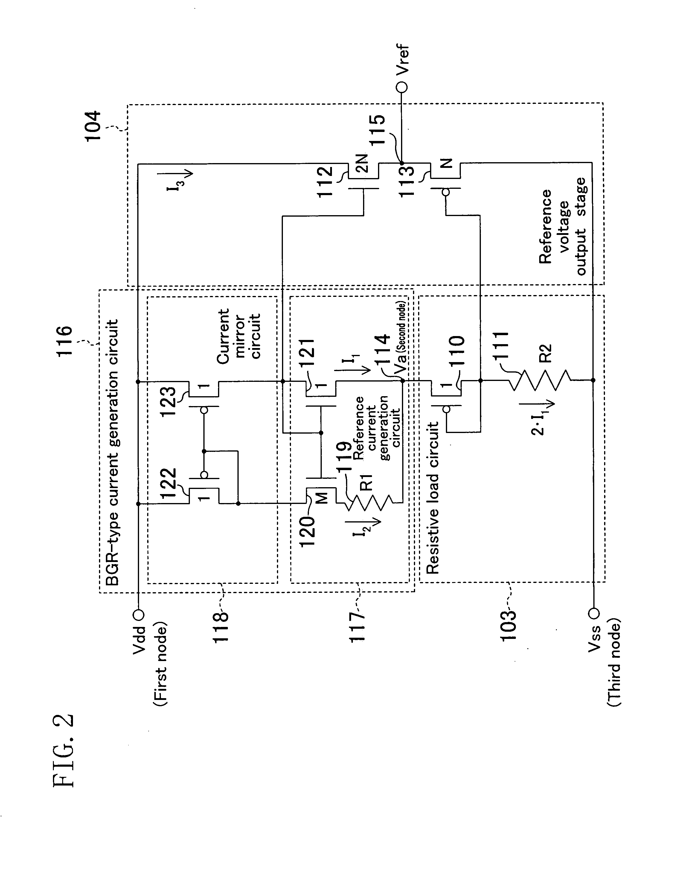
[0196]The reference voltage generation circuit of Embodiment 1 may be of a configuration as shown in FIG. 2. The reference voltage generation circuit of FIG. 2 includes a BGR-type current generation circuit 116, instead of the BGR-type current generation circuit 100 of FIG. 1.

[0197]The BGR-type current generation circuit 116 includes a reference current generation circuit 117 and a current mirror circuit 118.

[0198]The reference current generation circuit 117 includes a resistive element 119, and NMOS transistors 120 and 121 (the reference current MOS transistors) whose transistor size ratio is M:1.

[0199]The current mirror circuit 118 includes PMOS transistors 122 and 123 (the current mirror MOS transistors) designed so that an equal source-drain current flows therethrough.

[0200]The value M and the resistance values R1 and R2 of the resistive elements 119 and 111 are determined so as to satisfy Expression 8. Thus, ideally, the output voltage Vref is not varie...

embodiment 2

Variation of Embodiment 2

[0210]The reference voltage generation circuit of Embodiment 2 may be of a configuration as shown in FIG. 4. The reference voltage generation circuit of FIG. 4 includes the BGR-type current generation circuit 116, instead of the BGR-type current generation circuit 100 of FIG. 3.

[0211]The value M, the resistance values R1 and R2 of the resistive elements 119 and 202 are determined so that the portion in the braces in Expression 10 partially differentiated is zero.

[0212]Also with the configuration of FIG. 4 effects similar to those described above for the configuration of FIG. 3 are realized.

Embodiment 3

[0213]FIG. 5 is a circuit diagram showing a configuration of a reference voltage generation circuit according to Embodiment 3 of the present invention.

[0214]As shown in FIG. 5, the reference voltage generation circuit of the present embodiment includes a BGR-type current generation circuit 300, instead of the BGR-type current generation circuit 100 of the refer...

embodiment 3

Variation of Embodiment 3

[0233]The reference voltage generation circuit of Embodiment 3 may be of a configuration as shown in FIG. 6. The reference voltage generation circuit of FIG. 6 includes a BGR-type current generation circuit 307, instead of the BGR-type current generation circuit 300 of FIG. 5. The BGR-type current generation circuit 307 includes the current mirror circuit 118 and a reference current generation circuit 308. Moreover, the third node is connected to the drain-side power supply, and the first node is connected to the source-side power supply.

[0234]The reference current generation circuit 308 includes NMOS transistors 309 and 310 (the virtual short MOS transistors), diodes 311 and 312 (the reference current diodes), and a resistive element 313.

[0235]The NMOS transistors 309 and 310 are designed so that an equal source-drain current flows therethrough by, for example, using the same transistor size.

[0236]The diodes 311 and 312 are designed so that the diode size r...


PUM


Abstract

A reference voltage generation circuit of the present invention includes: a band gap reference-type current generation circuit for controlling each of currents flowing through a first current path and a second current path, which are extending from a first node to a second node, to be a predetermined reference current, by utilizing a voltage difference occurring between a pair of transistors or diodes; and a resistive load circuit provided between the second node and a third node.

Description

CROSS REFERENCE TO RELATED APPLICATION[0001]This application claims priority under 35 U.S.C. §119 on Patent Application No. 2006-188348 filed in Japan on Jul. 7, 2006, the entire contents of which are hereby incorporated by reference.BACKGROUND OF THE INVENTION[0002]1. Field of the Invention[0003]The present invention relates to a band gap reference-type reference voltage generation circuit for use in portable systems, battery-powered systems, integrated circuits provided therein, etc.[0004]2. Description of the Background Art[0005]A reference voltage generation circuit including a band gap reference circuit (referred also as a “BGR circuit”) is typically used in various analog circuits provided in semiconductor devices in order to suppress variations in the overall characteristics of the circuits due to variations in the power supply voltage and the temperature. A reference voltage obtained by means of such a BGR-type reference voltage generation circuit is known to be little depen...

Claims


Application Information

Patent Timeline
Patent Type & Authority Applications(United States)
IPC IPC(8): G05F3/16
CPCG05F3/30
Inventor MATSUMOTO, AKINORISAKIYAMA, SHIROMORIE, TAKASHI
Owner SOCIONEXT INC
Why Eureka
Try Eureka