Double-side process silicon mos and passive devices for RF front-end modules

a technology of silicon mos and front-end modules, applied in semiconductor devices, diodes, electrical apparatus, etc., can solve the problems of low signal to noise ratio (snr), large size, and many drawbacks of conventional rf front-end modules, and achieve low signal to noise ratio (snr), large size, and high power consumption

Active Publication Date: 2014-12-18
SEMICON MFG INT (SHANGHAI) CORP +1
View PDF4 Cites 40 Cited by
  • Summary
  • Abstract
  • Description
  • Claims
  • Application Information

AI Technical Summary

Benefits of technology

[0004]The inventors have observed that conventional RF front-end modules tend to suffer from many drawback, such as large size, low signal to noise ratio (SNR), higher power consumption, and other shortcomings. In addition, conventional system-level packaging methods tend to have high process complexity and high manufacturing cost.
[0005]Embodiments of the present invention provide an integrated circuit and associated processes for integrating components for RF front-end modules, including various transistors and different passive devices, on a single semiconductor substrate, utilizing both sides of the substrate. Depending on the embodiments, one or more of the following benefits can be achieved, such as smaller device size, higher signal-to-noise ratio, lower power consumption, etc., as compared with conventional methods. Further, the integrated process reduces the complexity and manufacturing cost of the RF system.

Problems solved by technology

The inventors have observed that conventional RF front-end modules tend to suffer from many drawback, such as large size, low signal to noise ratio (SNR), higher power consumption, and other shortcomings.
In addition, conventional system-level packaging methods tend to have high process complexity and high manufacturing cost.

Method used


Image

  • Double-side process silicon mos and passive devices for RF front-end modules
  • Double-side process silicon mos and passive devices for RF front-end modules
  • Double-side process silicon mos and passive devices for RF front-end modules

Examples


Embodiment Construction

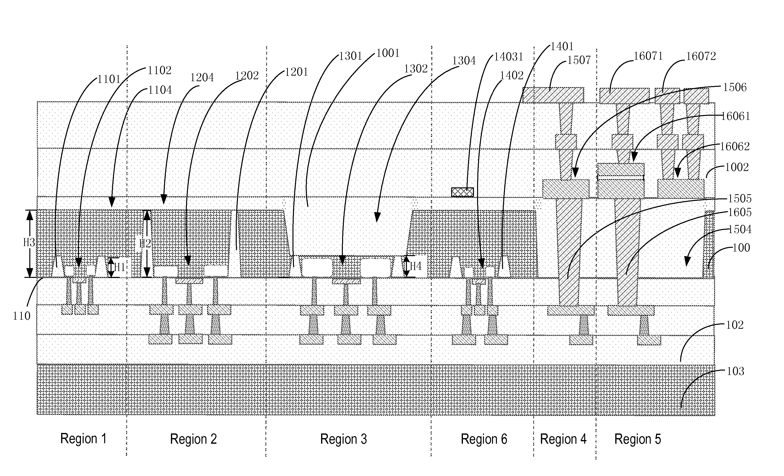
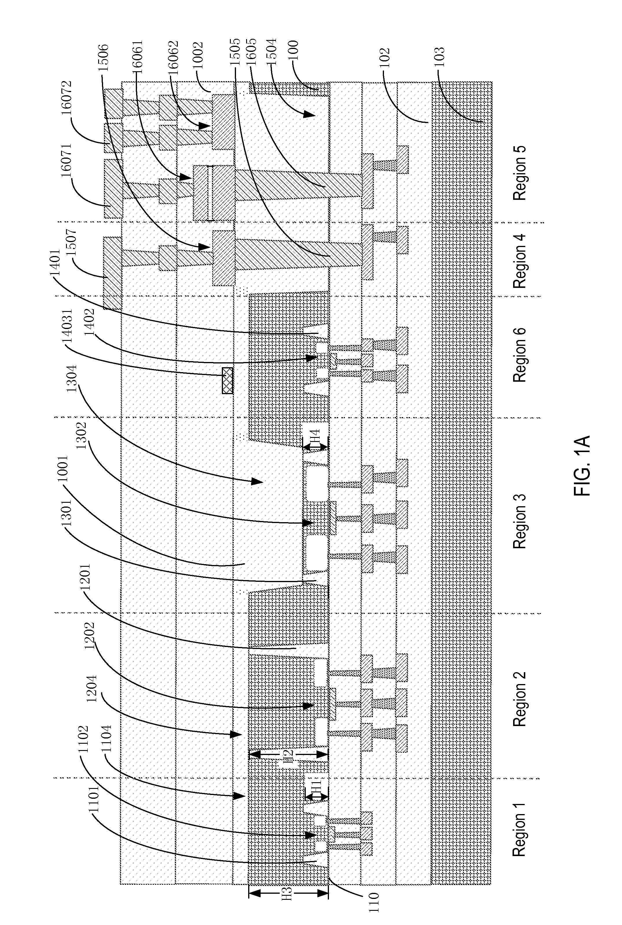
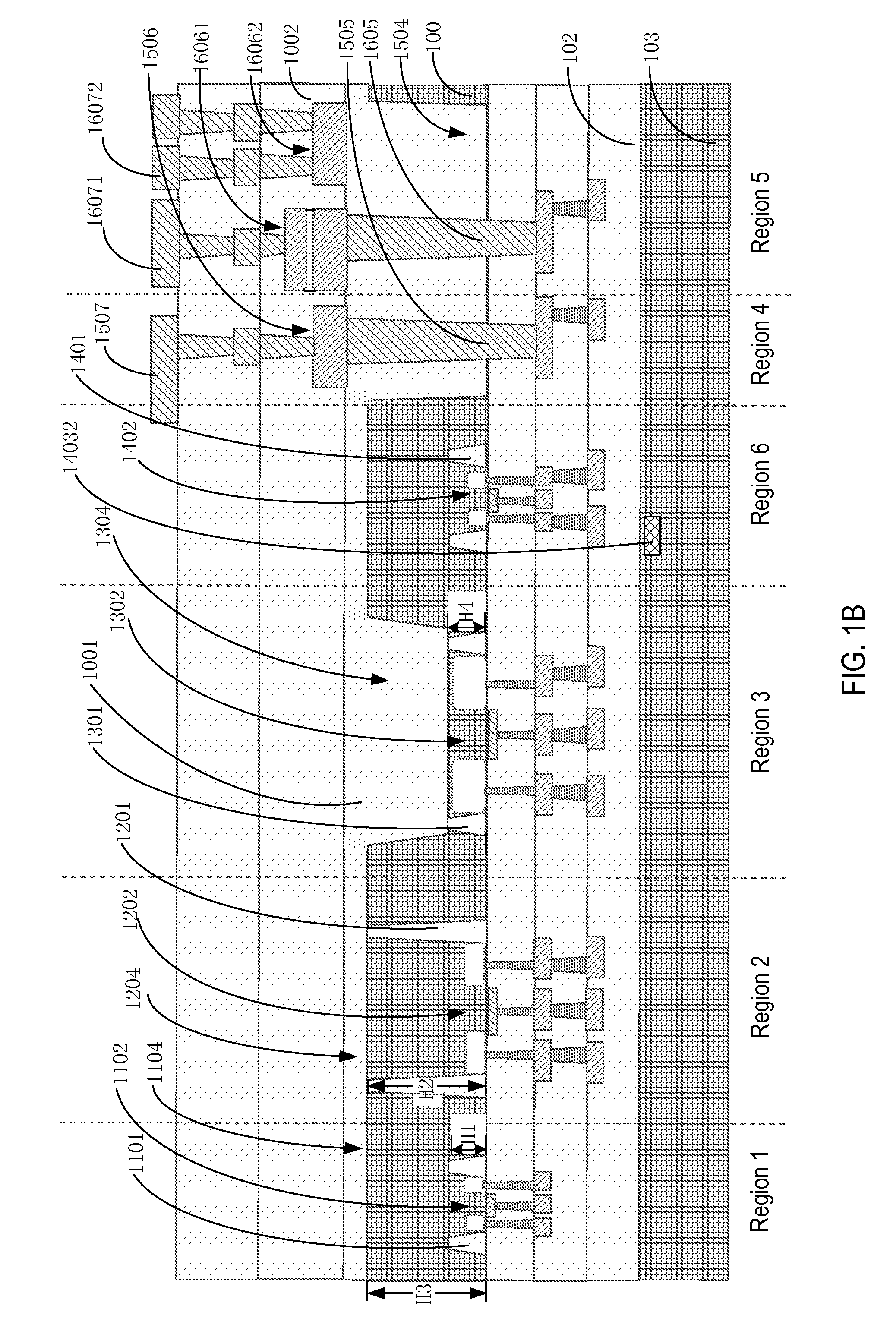
[0020]In the following description, numerous specific details are given in order to provide a more thorough understanding of the embodiments of the present invention. However, it is appreciated that one or more details can be omitted. In other examples, some technical characteristics known in the art are not described for simplicity. The preferred embodiment of the present invention is described below in detail, but the present invention can have other embodiments in addition to those described in detail.

[0021]It should be understood that in the drawings, for clarity, the relative dimensions of layers and regions may be altered. The same reference numerals are used to identify the same components throughout the disclosure, if possible.

[0022]It is also noted that when an element or layer is referred to as “on . . . the . . . ,”“adjacent to”, “connected to” or “coupled to” another element or layer, it can be directly on the other element or layer, adjacent, connected or coupled to the...


PUM


Abstract

A method for forming integrated circuit includes providing a first semiconductor substrate having a front surface and a back surface that is opposite to the front surface. One or more first trenches are in the first semiconductor substrate from the front surface side, the first trenches being characterized by a first depth. One or more second trenches are formed in the first semiconductor substrate from the front surface side, the second trenches being characterized by a second depth which greater than the first depth. A horizontal isolation layer is formed parallel to the front surface and at a third depth from the front surface. The method also includes forming a first recessed region extending in the first semiconductor substrate from the back surface side to the horizontal isolation layer that results in a thinned semiconductor region having a thickness substantially equal to the third depth. The method further includes forming a bulk dielectric layer covering the back surface side of the first semiconductor substrate.

Description

CROSS-REFERENCES TO RELATED APPLICATIONS[0001]This application claims priority to Chinese Patent Application No. 201310242363.1, filed Jun. 18, 2013, commonly owned and incorporated herein by reference in its entirety for all purposes.BACKGROUND OF THE INVENTION[0002]The present invention relates to semiconductor manufacturing processes. In particular, embodiments of the present invention relate to a method for forming integrated radio frequency frond-end modules.[0003]In the field of semiconductor technology, radio frequency frond-end module (RF FEM) is a key component in wireless communication devices, such as mobile phones, tablet computers, etc. In general, the RF front-end module typically includes components formed in different integrated circuit chips, such as chips for power amplifier core, power amplifier controller (PA controller), tuners RF, filters, duplexers, envelope tracking modules, etc. The amplifier core usually is made in a gallium arsenide (GaAs) chip or high vol...

Claims


Application Information

Patent Timeline
Patent Type & Authority Applications(United States)
IPC IPC(8): H01L21/762H01L27/06
CPCH01L27/0629H01L21/76251
Inventor HUANG, HERB HEDROWLEY, CLIFF
Owner SEMICON MFG INT (SHANGHAI) CORP
Why Eureka
Try Eureka