Display device and controlling method thereof

a technology of a display device and a control method, which is applied in the field of display devices, can solve the problems of high power consumption and heat generation of pixels, and achieve the effects of reducing heat generation and high power consumption at pixels, reducing deterioration of light emitting elements, and avoiding heat generation and high power consumption

Inactive Publication Date: 2007-02-20
SEMICON ENERGY LAB CO LTD
View PDF18 Cites 37 Cited by
  • Summary
  • Abstract
  • Description
  • Claims
  • Application Information

AI Technical Summary

Benefits of technology

[0033]As described above, the invention enables the driver transistor to operate in the saturation region without adding the deterioration margin (voltage α) to the setting voltage when the light emitting element starts emitting light. Therefore, the margin of the setting voltage due to the deterioration of the light emitting element is not needed anymore. In general, the voltage α for the deterioration margin is estimated at 2 to 6V, which causes the driving voltage to decrease as much. As a result, heat generation and high power consumption at pixels can be avoided. As heat generation of the driver transistor can be reduced particularly, the deterioration of the light emitting element can be reduced.

Problems solved by technology

The voltage applied to the cathode and anode of a light emitting element thus became inevitably high, causing heat generation and high power consumption.

Method used


Image

  • Display device and controlling method thereof
  • Display device and controlling method thereof
  • Display device and controlling method thereof

Examples


embodiment mode 1

[Embodiment Mode 1]

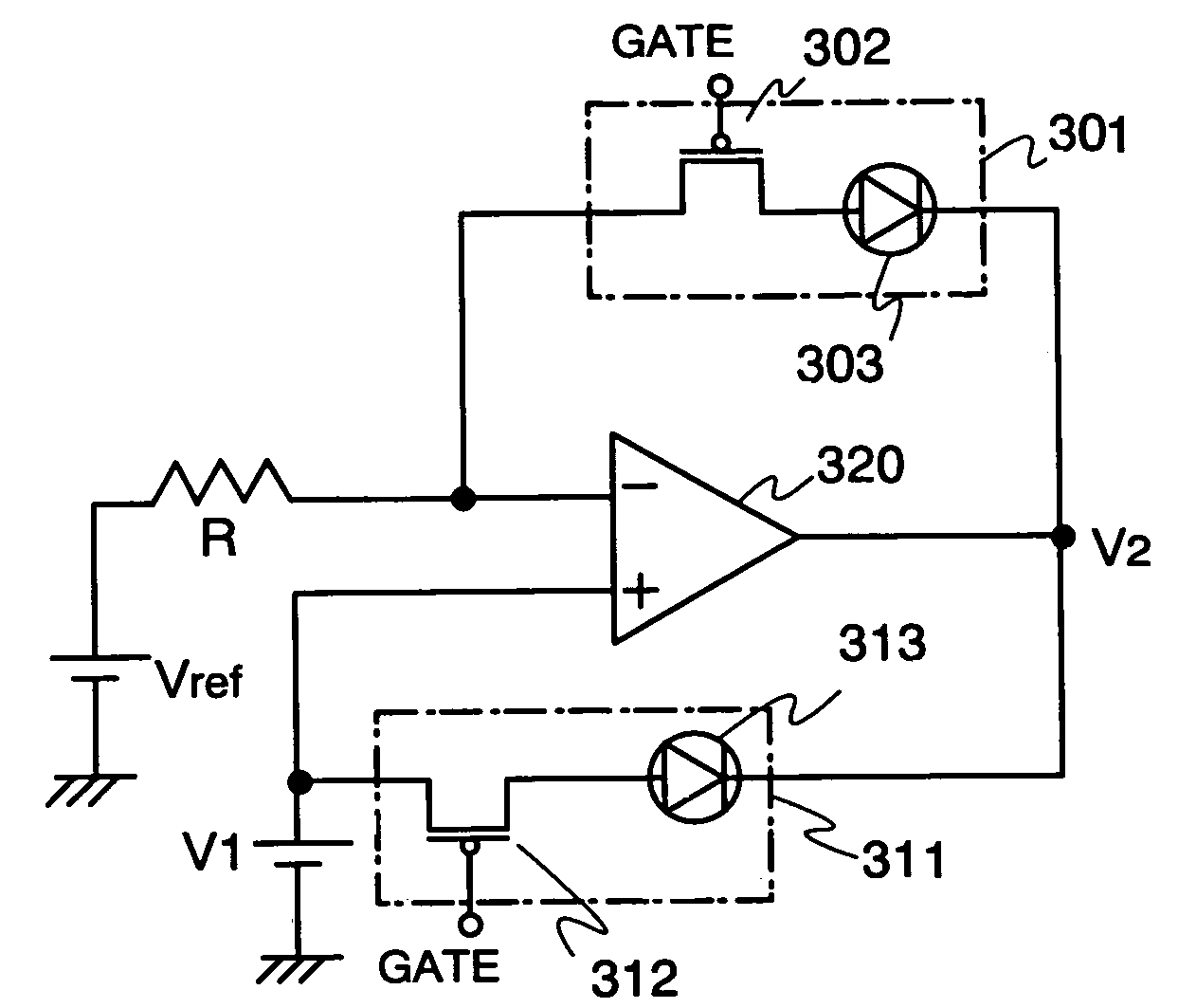
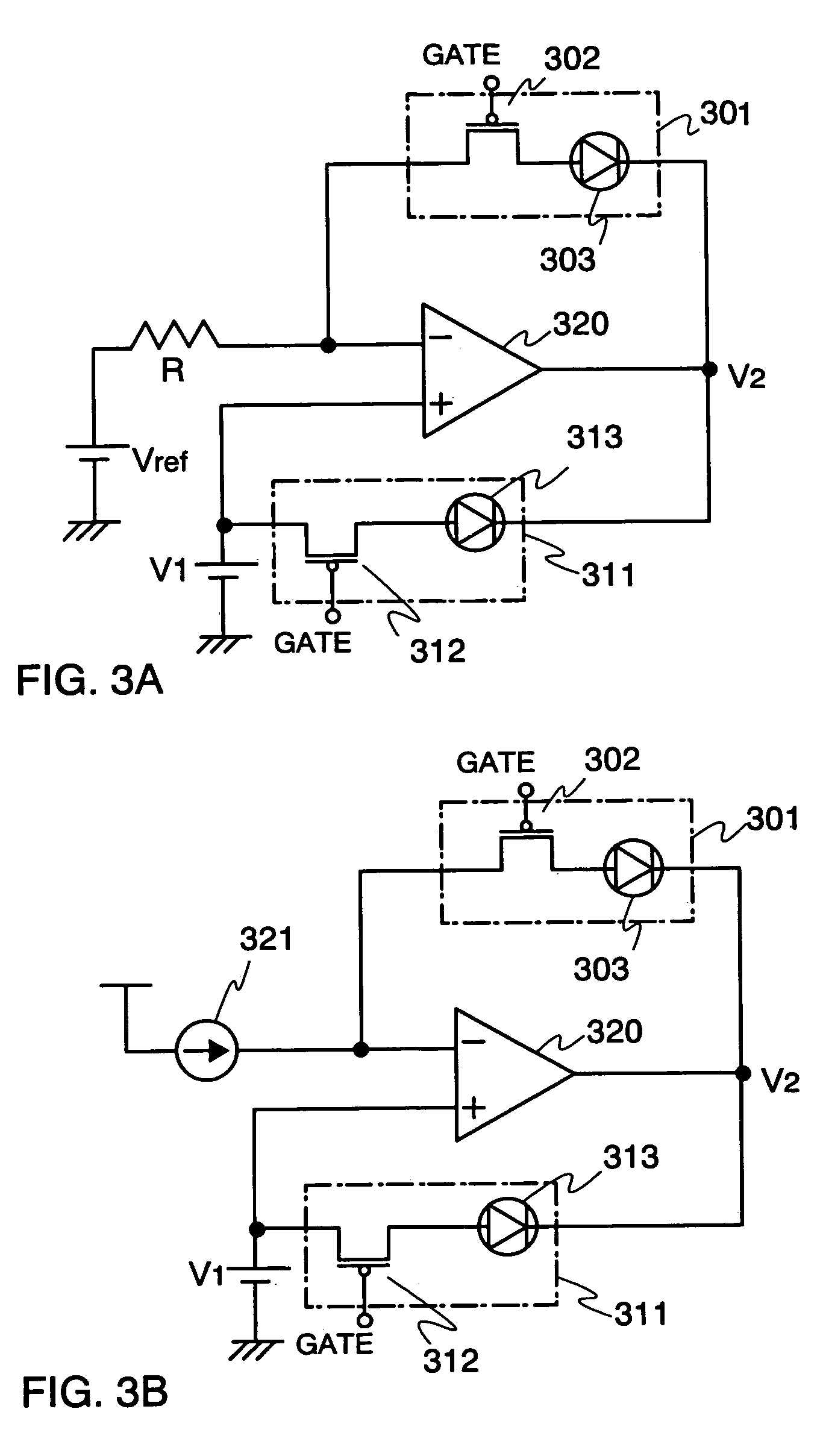
[0049]Hereinafter explained with reference to FIG. 3 is an example in which an operational amplifier is used as a power source voltage controller. Note that in this embodiment mode, a p-channel type driver transistor is applied, but an n-channel type driver transistor can be applied instead. Meanwhile, as an example of the invention, an anode potential of a pixel 311 (Vanode) is referred to as V1, and cathode potentials of the pixel 311 and of a monitoring element 301 (Vcathode) are referred to as V2.

[0050]FIG. 3A shows an equivalent circuit diagram of a pixel structure of the invention. A monitoring element 301 has a driver transistor 302 and a light emitting element 303 which is connected to a second electrode of the driver transistor 302. A pixel 311 has a driver transistor 312 and a light emitting element 313 which is connected to a second electrode of the driver transistor 312. The light emitting elements 303 and 313 are connected to an output terminal of the...

embodiment mode 2

[Embodiment Mode 2]

[0070]Hereinafter explained with reference to FIG. 4 is a different pixel structure from that of Embodiment Mode 1. Note that in this embodiment mode, a driver transistor is a p-channel type, an anode potential of a light emitting element (Vanode) is referred to as V1, and a cathode potential of the light emitting element (Vcathode) is referred to as V2.

[0071]An equivalent circuit diagram of a pixel structure is shown in FIG. 4. As well as Embodiment Mode 1, a monitoring element 401 has a driver transistor 402 and a light emitting element 403 which is connected to a second electrode of the driver transistor 402. A pixel 411 has a driver transistor 412 and a light emitting element 413 which is connected to a second electrode of the driver transistor 412. The light emitting elements, 403 and 413 are connected to an output terminal of the operational amplifier 420 and have a voltage of V2. Meanwhile, first electrodes of the driver transistors 402 and 412 have potenti...

embodiment mode 3

[Embodiment Mode 3]

[0081]Hereinafter explained is a different pixel structure from those of Embodiment Mode 1 and Embodiment Mode 2.

[0082]FIG. 10 shows a circuit diagram as described in Embodiment Mode 2, wherein a switching regulator 3000 is applied in stead of an operational amplifier as a power source voltage controller. For a constitution where an operational amplifier is applied, a power source circuit for the operational amplifier is required. This embodiment mode makes it possible to unite an operational amplifier and the power source circuit by using a switching regulator.

[0083]A pixel structure which has a switching regulator will be hereinafter described. In FIG. 10, the switching regulator 3000 is comprised of an error amplifier 3001, a PWN comparator 3002, a reference power sources 3003 and 3010, an oscillation circuit 3004, a switching transistor 3008, an inductor 3009, a diode 3006, a smoothing capacitor 3005 and a battery 3007. As well as Embodiment Mode 2, a monitori...


PUM


Abstract

A conventional setting voltage was a value with an estimated margin of a characteristic change of a light, emitting element. Therefore, a voltage between the source and drain of a driver transistor Vds had to be set high (Vds≧Vgs−VTh+a). This caused high heat generation and power consumption, because a voltage applied to the light emitting element. The invention is characterized by, feedbacking a change in a current value in accordance with the deterioration of a light emitting element and a power source voltage controller which modifies a setting voltage. Namely, according to the invention, the setting voltage is to be set in the vicinity of the boundary (critical part) between, a saturation region and a linear region, and a voltage margin for the deterioration is not required particularly for an initial setting voltage.

Description

BACKGROUND OF THE INVENTION[0001]1. Field of the Invention[0002]The present invention relates to a display device (light emitting device) having a light emitting element, and more particularly such a display device having a display part of current driving method.[0003]2. Description of the Related Art[0004]Digital gradation method (digital driving method) and analog gradation method (analog driving method) can be given as driving method of multi-color expression on a display device having a light emitting element. In the aforementioned digital gradation method, a light emitting element is driven in binary of ON (brightness is almost 100%),and OFF (brightness is almost 0%) to obtain gradation by controlling the luminous region and the length of the period during which each pixel emits light. In the analog gradation method, analog input data is written into a light emitting element to modulate the gradation in an analog manner.[0005]Furthermore, expression of gradation is made through...

Claims


Application Information

Patent Timeline
Patent Type & Authority Patents(United States)
IPC IPC(8): G09G5/00G09G3/32
CPCG09G3/3233H01L27/124G09G2300/0426G09G2300/0842G09G2300/0861G09G2310/0251G09G2320/0295G09G2320/043G09G2330/021G09G2330/028G09G2320/029G09G3/20G09G3/30
Inventor MIYAGAWA, KEISUKEKOYAMA, JUN
Owner SEMICON ENERGY LAB CO LTD
Why Eureka
Try Eureka