
Device testing architecture, method, and system

a technology of device testing and testing method, applied in the direction of electronic circuit testing, measurement device, instruments, etc., can solve the problems of tester cost problem that is significantly worsening, and the standard does not provide standardization of such circuits

Active Publication Date: 2008-01-10
TEXAS INSTR INC
View PDF4 Cites 11 Cited by
  • Summary
  • Abstract
  • Description
  • Claims
  • Application Information

AI Technical Summary

Benefits of technology

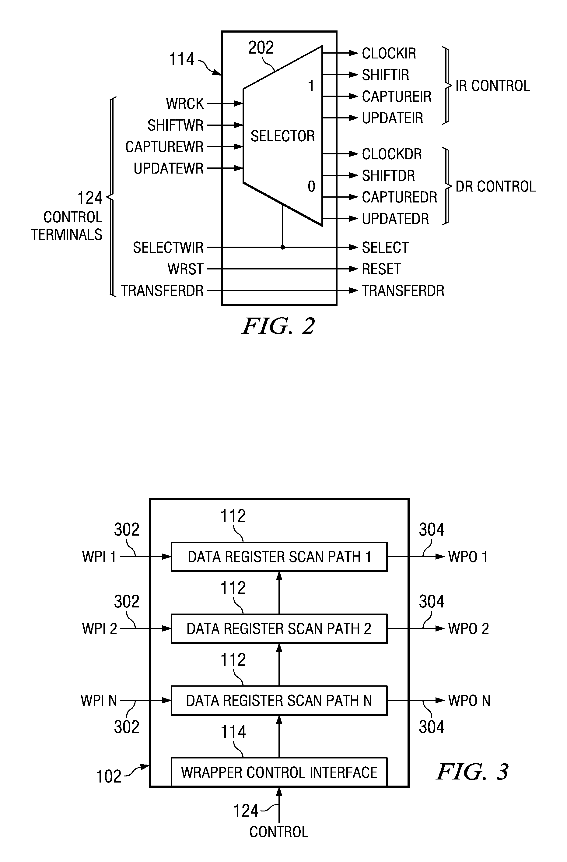
[0009]The present disclosure provides a device test architecture, interface, and method for enabling efficient testing of large numbers of devices simultaneously. The device test architecture internally evaluates the test response using a compare circuit within the device, which eliminates the need to output the device test response to the tester. The disclosures ability to evaluate test response inside the devices simplifies testers to only having to input test data and control to the device. The device test architecture includes a programmable test controller that can be programmed by an instruction to perform any number of test operations without having to increase the number of signals on the test interface.

Problems solved by technology

The tester cost problem worsens significantly when multiple DUTs 502 need to be tested simultaneously, such as at wafer level testing where multiple die (DUTs) need to be contacted and simultaneously tested to reduce semiconductor manufacturing cost.
User defined TAMs are mentioned in IEEE standard 1500, but the standard does not provide standardization of such circuits.

Method used


Image

  • Device testing architecture, method, and system
  • Device testing architecture, method, and system
  • Device testing architecture, method, and system

Examples


Embodiment Construction

[0055]FIG. 7 illustrates a preferred embodiment of the testing method, testing apparatus, and testing system as disclosed in the present disclosure. The embodiment includes a DUT 702 test architecture, a DUT tester 712, and a DUT to tester interface 714 including an input bus 720, a control bus 722, a scan input 724 and a scan output 726. While not shown and as mentioned previously in regard to FIG. 5, the DUT will also have a test enable input from the tester that is used to switch the DUT from its functional architectural configuration into the test architectural configuration shown in FIG. 7. The DUT test architecture includes a TAM 704 for each embedded core 708, a TAM controller 706 for each embedded core 708, a TAM selector 710 for selecting an embedded core's TAM 704 and TAM controller 706, and a scan router 744 for routing the flow of serial data between tester 712 and various TAM controllers 706. Each embedded core 708 includes an IEEE 1500 wrapper architecture 102 and inte...


PUM


Abstract

A device test architecture and interface is provided to enable efficient testing embedded cores within devices. The test architecture interfaces to standard IEEE 1500 core test wrappers and provides high test data bandwidth to the wrappers from an external tester. The test architecture includes compare circuits that allow for comparison of test response data to be performed within the device. The test architecture further includes a memory for storing the results of the test response comparisons. The test architecture includes a programmable test controller to allow for various test control operations by simply inputting an instruction to the programmable test controller from the external tester. The test architecture includes a selector circuit for selecting a core for testing. Additional features and embodiments of the device test architectures are also disclosed.

Description

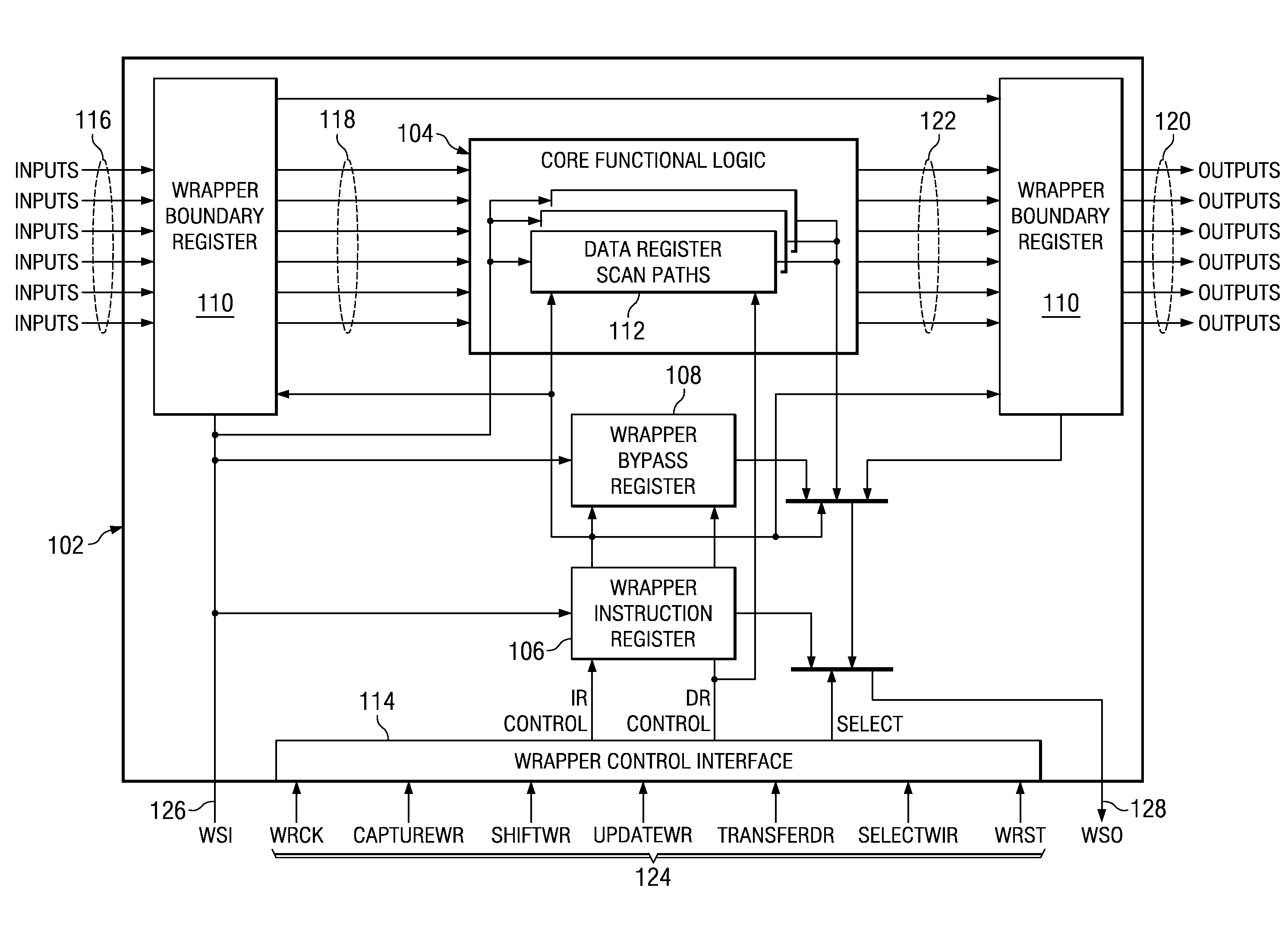
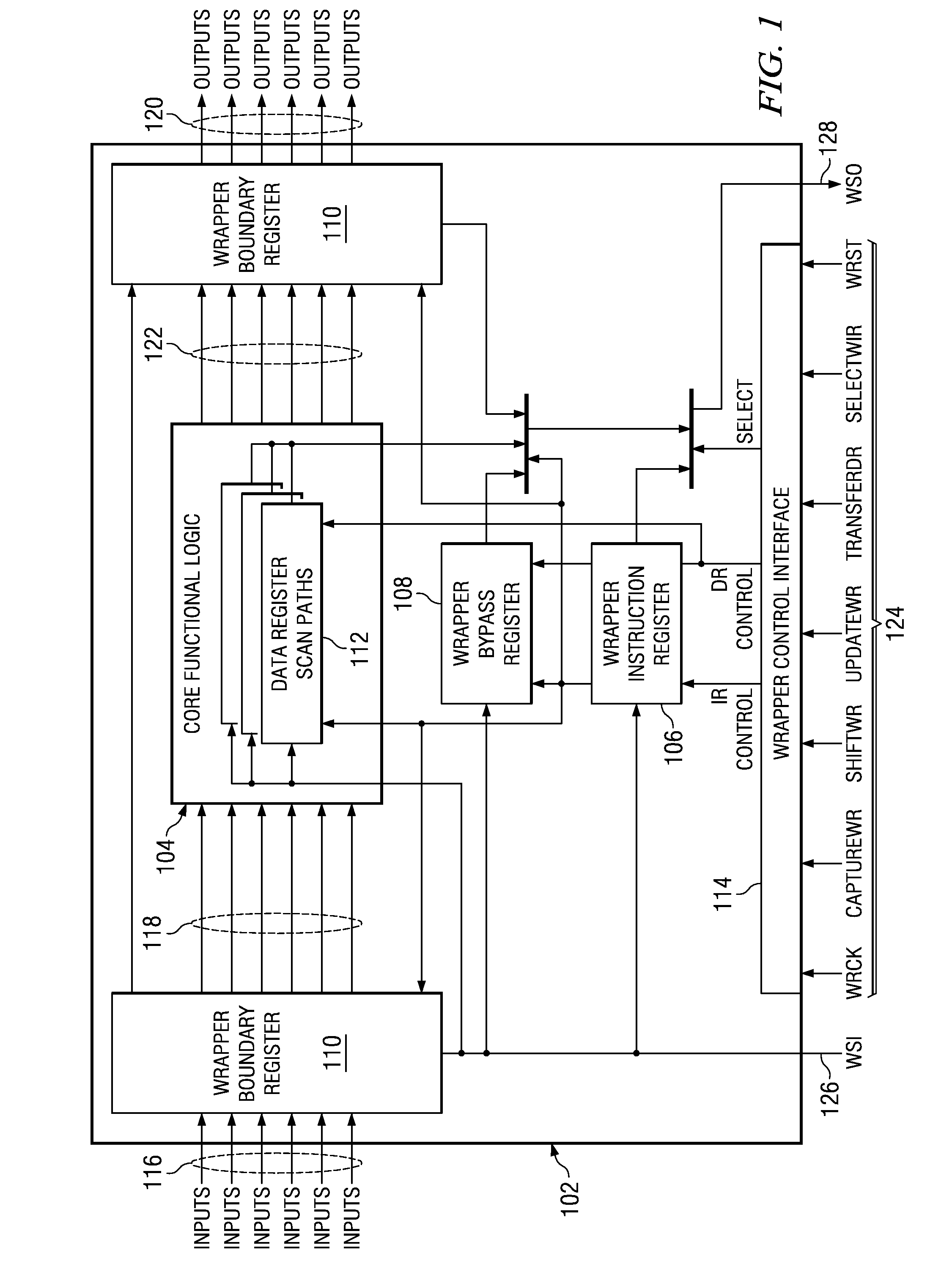
[0001]This application claims priority from Provisional Application No. 60 / 804,962, filed on Jun. 16, 2006.FIELD OF THE DISCLOSUREDescription of Related Art[0002]FIG. 1 illustrates the test wrapper architecture 102 defined in IEEE standard 1500. The wrapper architecture is used to perform internal testing of a core circuit 104 embedded within and integrated circuit. The wrapper architecture is also used to perform external testing of the interconnects to other embedded core circuits connected to the embedded core circuit 104. The wrapper architecture is very similar to the boundary scan test architecture defined in IEEE 1149.1, in that it includes: (1) a wrapper instruction register (WIR) 106 for storing test instructions, (2) a wrapper bypass register (WBY) 108 for providing an abbreviated scan path through the wrapper, and a wrapper boundary register (WBR) 110 for controlling the core outputs, controlling the core inputs, observing the core outputs, and observing the core inputs. ...

Claims


Application Information

Patent Timeline
Patent Type & Authority Applications(United States)
IPC IPC(8): G01R31/28
CPCG01R31/318555G01R31/3177G01R31/318563
Inventor WHETSEL, LEE D.
Owner TEXAS INSTR INC
Learn More