
Method of manufacturing a sticker type antenna

a technology of sticker antenna and manufacturing method, which is applied in the direction of conductive pattern formation, burglar alarm mechanical actuation, instruments, etc., can solve the problems of high cost and poor competition of sticker antenna, and achieve the effect of increasing the relative distance between mylar and saving manpower

Inactive Publication Date: 2008-01-17
AUDEN TECHNO
View PDF7 Cites 13 Cited by
  • Summary
  • Abstract
  • Description
  • Claims
  • Application Information

AI Technical Summary

Benefits of technology

[0006]The present invention primarily is to provide a method of manufacturing a sticker type antenna, in which a copper foil of 0.017 mm by thickness is stuck to a layer of releasable film in advance, in order that the copper foil can bear the pulling force in the brush electroplating process to thereby substitute the conventional beryllium copper of 0.1 mm by thickness, and to largely reduce the cost of production, the antenna made is much thinner than an antenna of the same style.
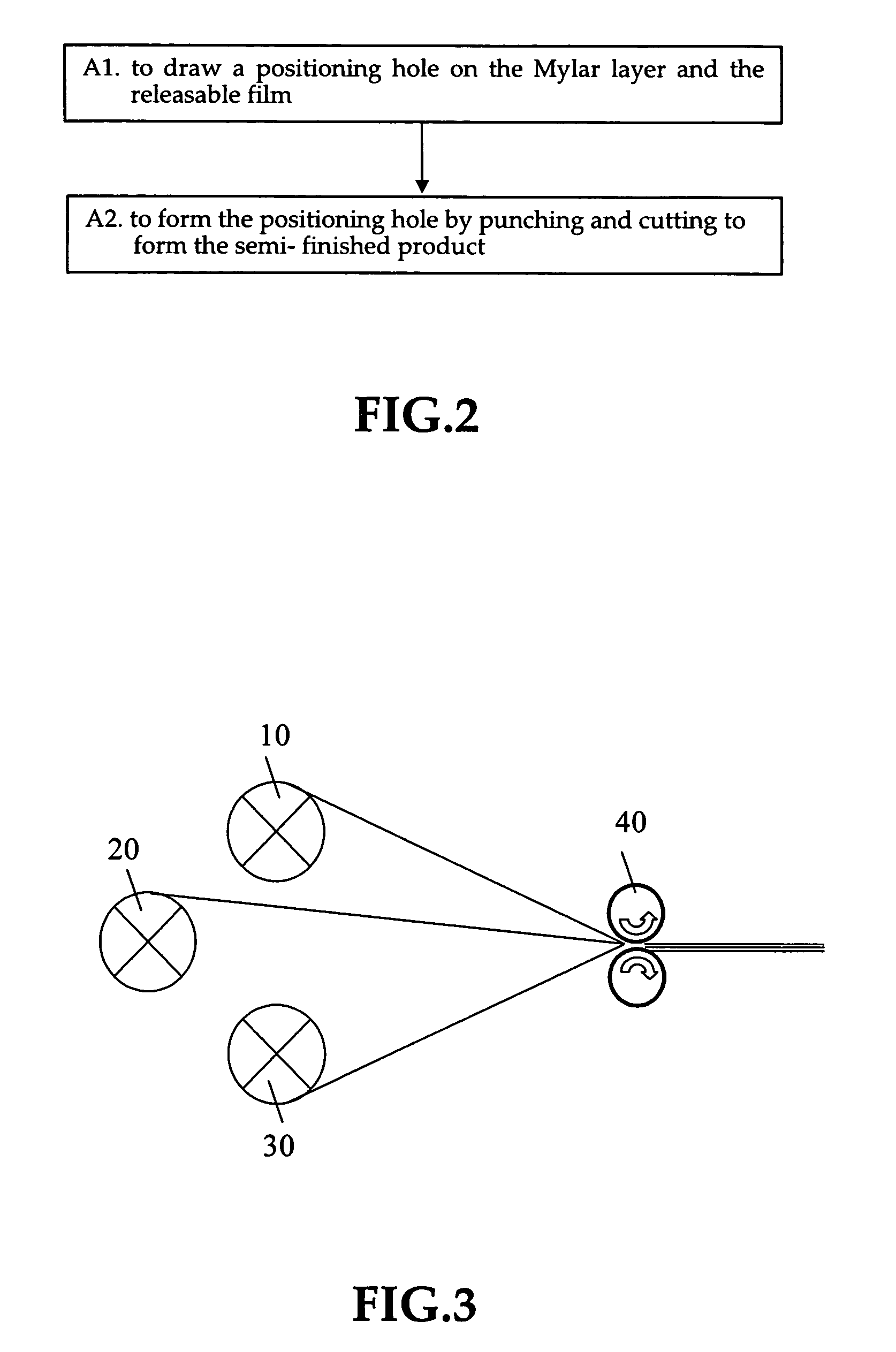
[0009]And in the manufacturing method of the present invention, the releasable film and the Mylar layer are punched with a positioning hole to allow manipulation of an automatized machine on an alignment point during the manufacturing process, this can save consumption of manpower and increase the stability of the relative distance between the Mylar and the copper foil.
[0010]Moreover, punching a positioning hole on the product of antenna of the present invention can allow a customer to stick the antenna on the main body of a mobile phone or a mobile electronic device.

Problems solved by technology

By virtue that the price of beryllium copper is high, the cost of a sticker type antenna is high consequently, this is not good for competition.

Method used


Image

  • Method of manufacturing a sticker type antenna
  • Method of manufacturing a sticker type antenna
  • Method of manufacturing a sticker type antenna

Examples


Embodiment Construction

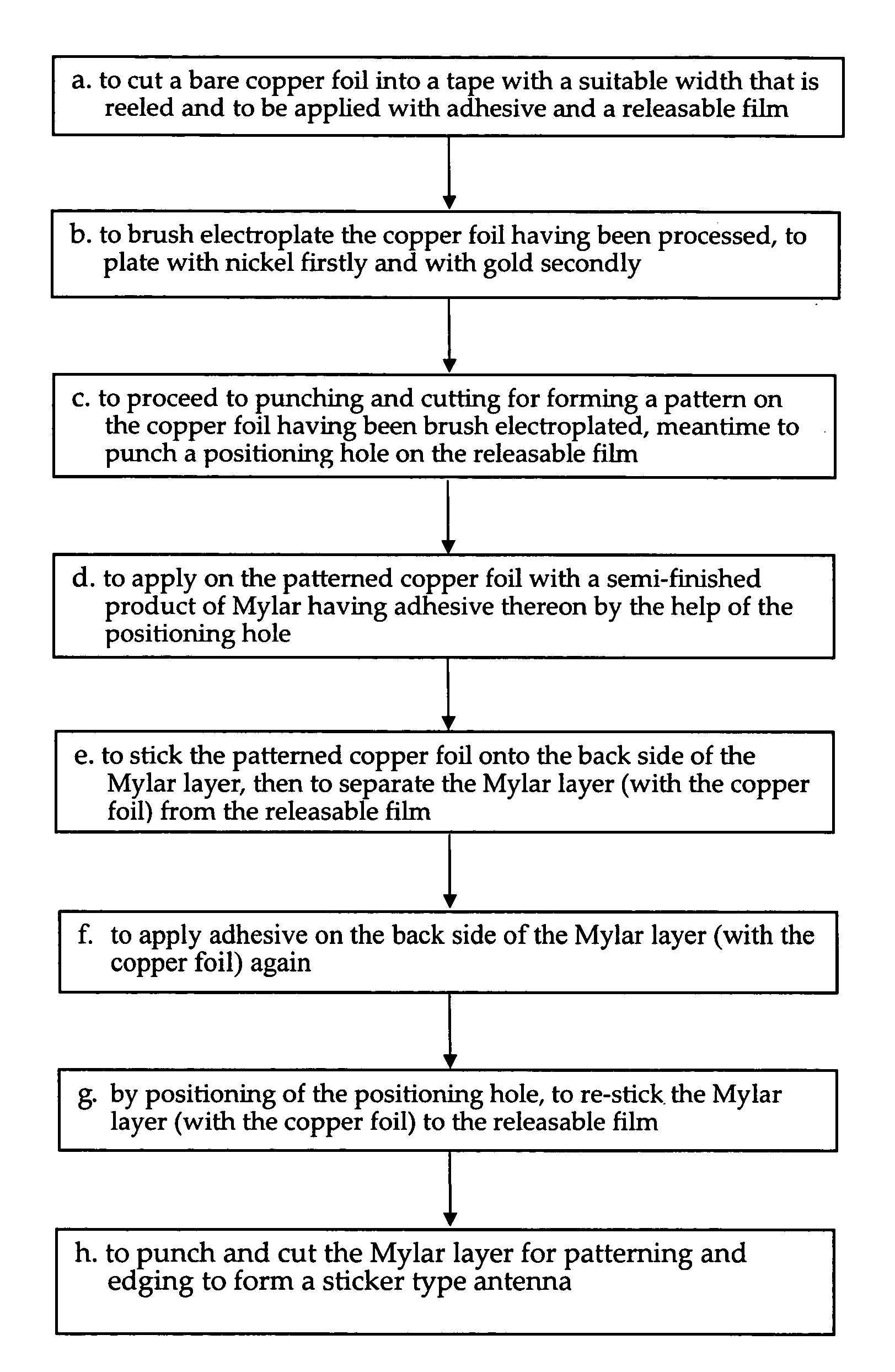
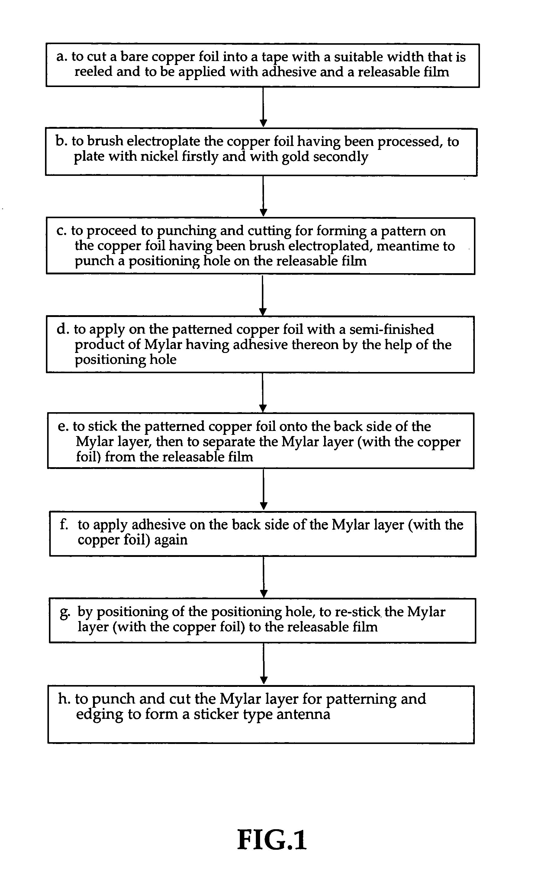
[0016]Referring firstly to FIG. 1 which is a process flowchart of the method of manufacturing of the present invention, it includes the steps of:[0017]a. to cut a bare copper foil into a tape with a suitable width that is reeled and to be applied with adhesive and a releasable film;[0018]b. to brush electroplate the copper foil having been processed, to plate with nickel firstly and with gold secondly;[0019]c. to proceed to punching and cutting for forming a pattern on the copper foil having been brush electroplated, meantime to punch a positioning hole on the releasable film;[0020]d. to apply on the patterned copper foil with a semi-finished product of Mylar having adhesive thereon by the help of the positioning hole;[0021]e. to stick the patterned copper foil onto the back side of the Mylar layer, then to separate the Mylar layer (with the copper foil) from the releasable film;[0022]f. to apply adhesive on the back side of the Mylar layer (with the copper foil) again; and[0023]g. ...


PUM

PropertyMeasurementUnit
Thicknessaaaaaaaaaa

Abstract

A method of manufacturing a sticker type antenna, in which a copper foil of 0.017 mm by thickness is stuck to a layer of releasable film in advance, in order that the copper foil can bear the pulling force in a brush electroplating process to thereby substitute the conventional beryllium copper of a larger thickness. The copper foil after brush electroplating undergoes punching and cutting for forming a pattern and is stuck to a semi-finished product of Mylar, hence the copper foil is stuck onto the back side of the Mylar layer; then the Mylar layer with the copper foil is separated from the releasable film, then the back side of the Mylar layer is applied with adhesive and again is stuck to the releasable film; after punching and cutting the Mylar layer for patterning and edging, a sticker type antenna is made.

Description

BACKGROUND OF THE INVENTION [0001]1. Field of the Invention[0002]The present invention relates to a method of manufacturing a sticker type antenna, and especially to a method of manufacturing a sticker type antenna of a copper foil of 0.017 mm by thickness.[0003]2. Description of the Prior Art[0004]A sticker type antenna is convenient for being loaded in a minimized mobile phone or a mobile electronic device. Manufacturing of a conventional sticker type antenna uses beryllium copper of 0.1 mm by thickness, because only beryllium copper of such a thickness can bear the pulling force required in the subsequent brush electroplating process. By virtue that the price of beryllium copper is high, the cost of a sticker type antenna is high consequently, this is not good for competition.[0005]And more, a sticker type antenna must be enveloped with a layer of Mylar (a kind of polyester film) for protection, however, the Mylar is only stuck to copper in the process of manufacturing, it happen...

Claims


Application Information

Patent Timeline
IPC IPC(8): H01P11/00
CPCH01Q1/00H01Q1/243H05K3/041H05K3/241H05K3/244Y10T29/49155H05K2201/0355H05K2203/0156H05K2203/1545Y10T29/49016Y10T29/49128H05K3/386
Inventor LIN, CHUN-WEIHUANG, TUNG-LIANG
Owner AUDEN TECHNO
Learn More