Ecc system for memory

Active Publication Date: 2008-01-17
TAIWAN SEMICON MFG CO LTD
View PDF8 Cites 57 Cited by
  • Summary
  • Abstract
  • Description
  • Claims
  • Application Information

AI Technical Summary

Benefits of technology

[0017] According to an embodiment of the present aspect, each of said second columns of the parity array are distributed in said memory array for dividing the memory array into at least the two sub-arrays. Each of said second columns is located at a position for minimizing a wiring distance between each of said second columns and logic elements of the ECC logic circuitry for receiving parity data bits provided by said second columns. In an alternate embodiment, groups of said second columns of the parity array are distributed in said memory array for dividing the memory array into at least the two sub-arrays. Each of said groups of second columns includes at least two adjacent second columns, the at least two adjacent second columns being located at a position for minimizin

Problems solved by technology

Those skilled in the art will understand that long wires results in extra resistive capacitive (RC) delay, thereby limiting ECC performance as the circuitry must wait for the slowest parity bit to arrive before executing ECC operations.
Also, increased capacitance results in increased power consumption.
Those skilled in the art will understand that anomalies during semiconductor fabrication can cause such defects in the memory

Method used


Image

  • Ecc system for memory
  • Ecc system for memory
  • Ecc system for memory

Examples


Embodiment Construction

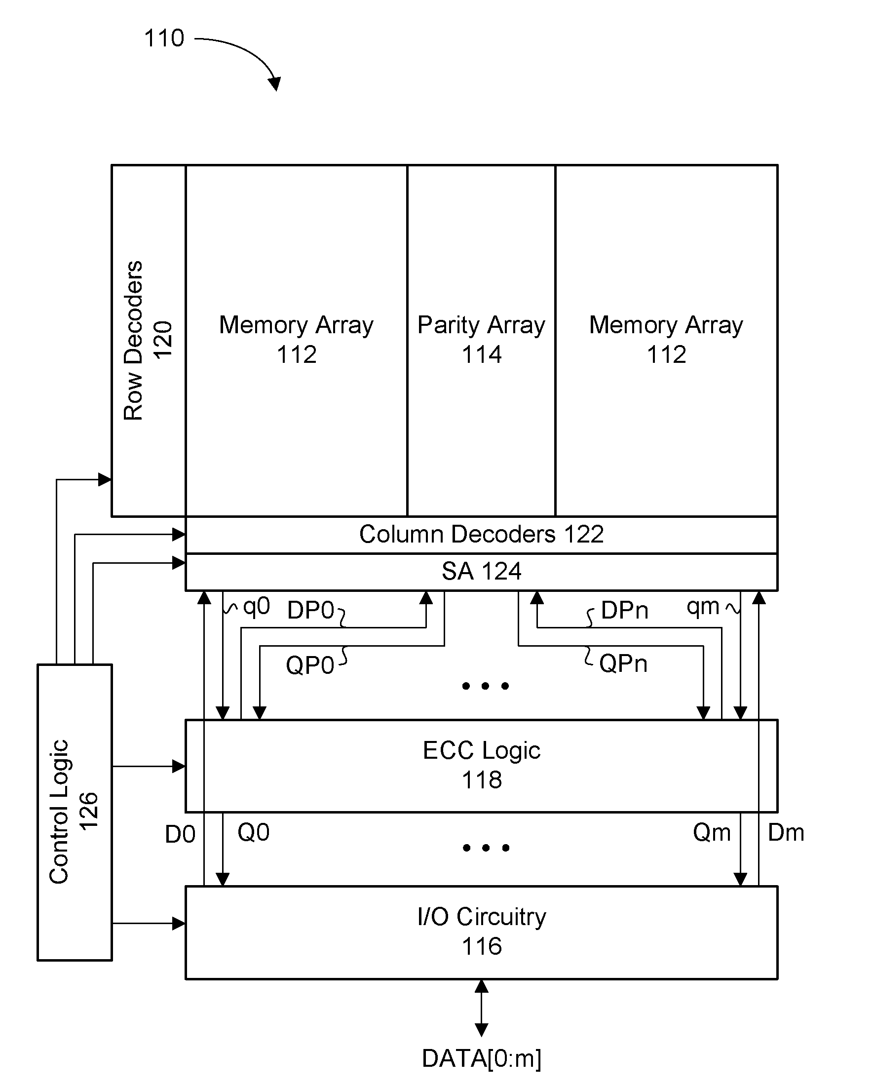
[0033] An error correction code system for a memory for improving performance and testability is described. The parity columns of the memory array can be positioned centrally within the array to minimize routing distance to ECC logic circuitry. The parity columns can be grouped together or distributed throughout the array to optimize performance. A multiplexor circuit can be included for selectively coupling the parity bits stored in the parity memory array to one or more external pins. Therefore, the parity columns can be directly tested, and testing of the ECC logic circuitry is facilitated.

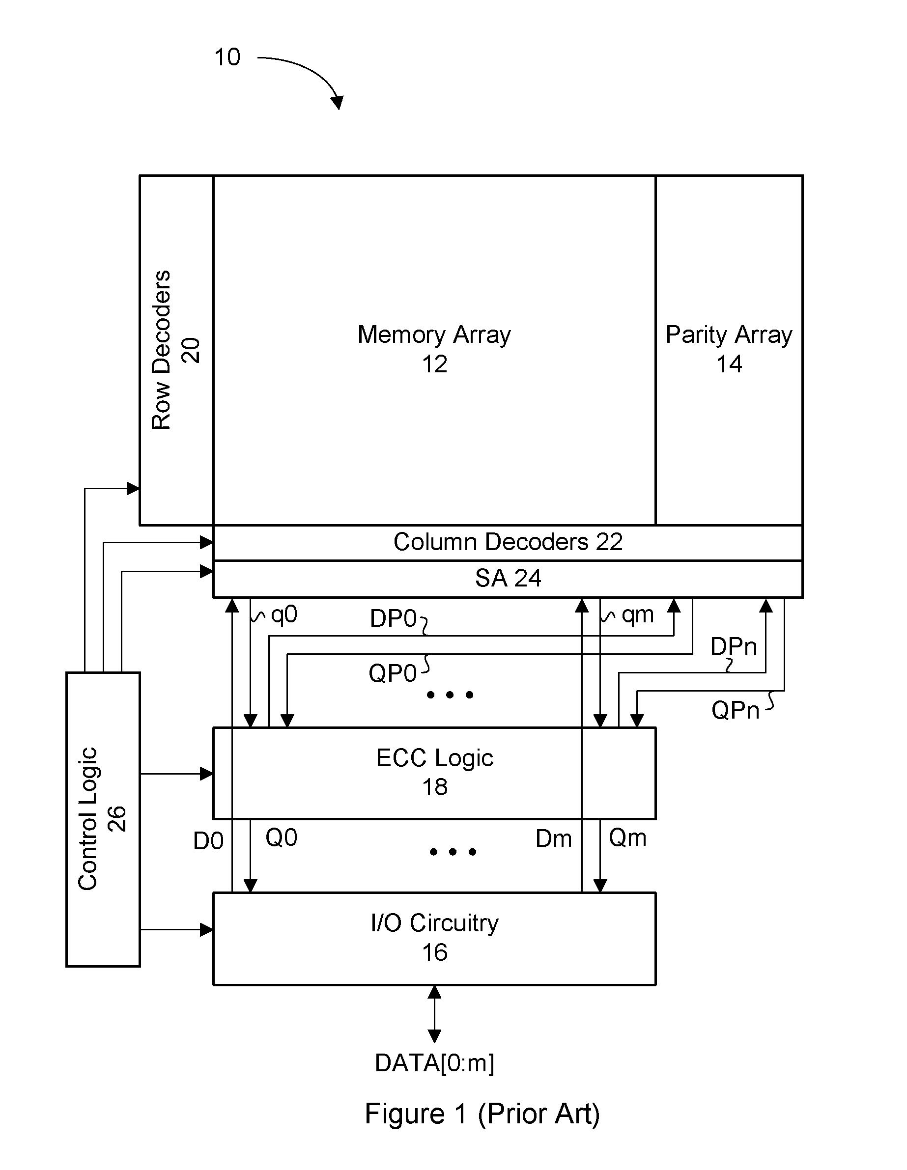
[0034] Reference is made to FIG. 3 which shows a block diagram of a memory with an ECC system according to an embodiment of the present invention. To simplify the description, the numerals used previously in describing FIG. 1, will be used again after raising the numerals by 100 where circuit elements to be described share similarities with circuit elements already described. The memory with t...


PUM


Abstract

An error correction code system for a memory for improving performance and testability. The parity columns of the memory array can be positioned centrally within the array to minimize routing distance to ECC logic circuitry. The parity columns can be grouped together or distributed throughout the array to optimize performance. A multiplexor circuit can be included for selectively coupling only the parity bits stored in the parity memory array to I/O circuitry. Therefore, the parity columns can be directly tested, and testing of the ECC logic circuitry is facilitated.

Description

CROSS REFERENCE TO RELATED APPLICATIONS [0001] This application claims the benefit of priority of U.S. Provisional Patent Application No. 60 / 805,814 filed on Jun. 26, 2006, which is incorporated herein by reference in its entirety.FIELD OF THE INVENTION [0002] The present invention relates to error correction code (ECC) systems for semiconductor memories. BACKGROUND OF THE INVENTION [0003] Historically, ECC has been used to correct errors that occur within data patterns provided by semiconductor memories, such as DRAM, SRAM and non-volatile memories. As will be appreciated by those skilled in the art, this involves creating and storing extra bits known as parity bits. The extra data bits required for the ECC (parity bits) are appended to the data or memory. Typically semiconductor memories (both discrete and embedded) have used ECC to correct soft errors caused by radiation. [0004] Typically for every 32 bits of data at least 6 extra bits of data are required. These 6 extra bits of ...

Claims


Application Information

Patent Timeline
IPC IPC(8): G06F11/20
CPCG06F11/1048
Inventor EARL, ADRIANRAO, RAVIPRAKRASH S.JOSHI, VINEET
Owner TAIWAN SEMICON MFG CO LTD
Why Eureka
Try Eureka