Touch panel

a touch panel and display device technology, applied in the field of touch panels, can solve the problems of poor visibl of the liquid crystal display device on the rear face of the touch panel, degrade the piezoelectric material, and difficulty in manufacturing

Inactive Publication Date: 2008-01-24
PANASONIC INTELLECTUAL PROPERTY MANAGEMENT CO LTD
View PDF4 Cites 25 Cited by
  • Summary
  • Abstract
  • Description
  • Claims
  • Application Information

AI Technical Summary

Problems solved by technology

As a result, a fringe pattern of light, a so-called Newton ring, is generated, and the liquid crystal display device on the rear...

Method used


Image

  • Touch panel
  • Touch panel
  • Touch panel

Examples


embodiment

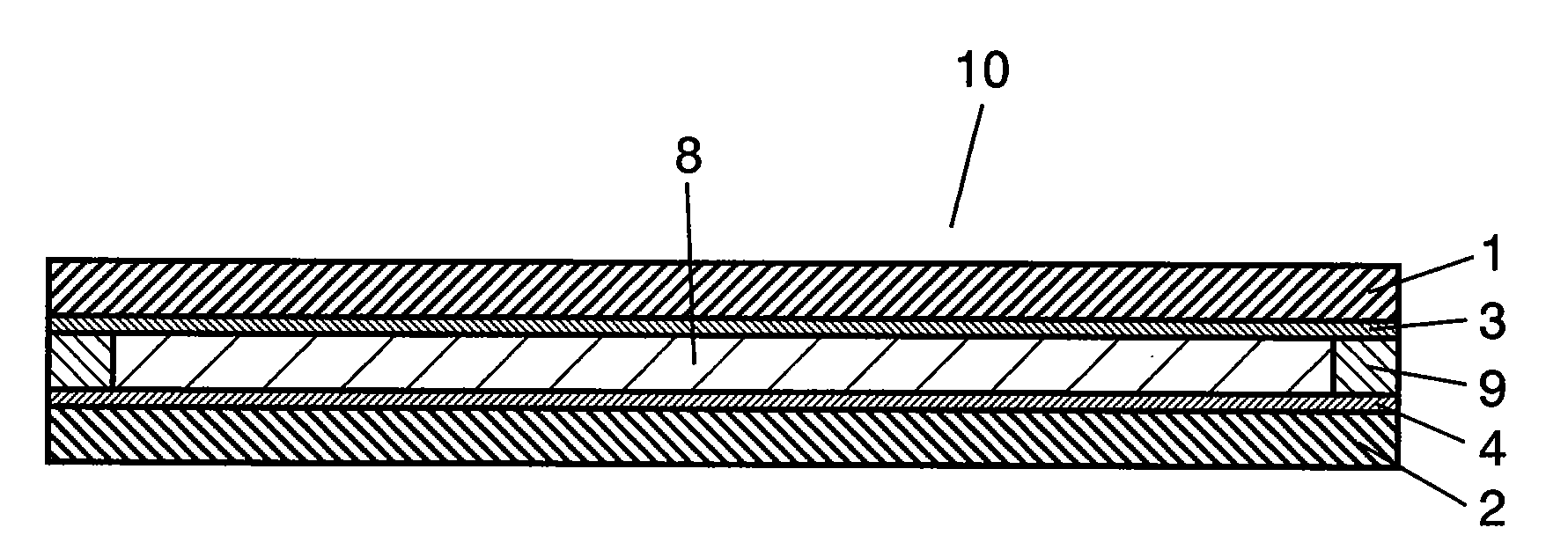
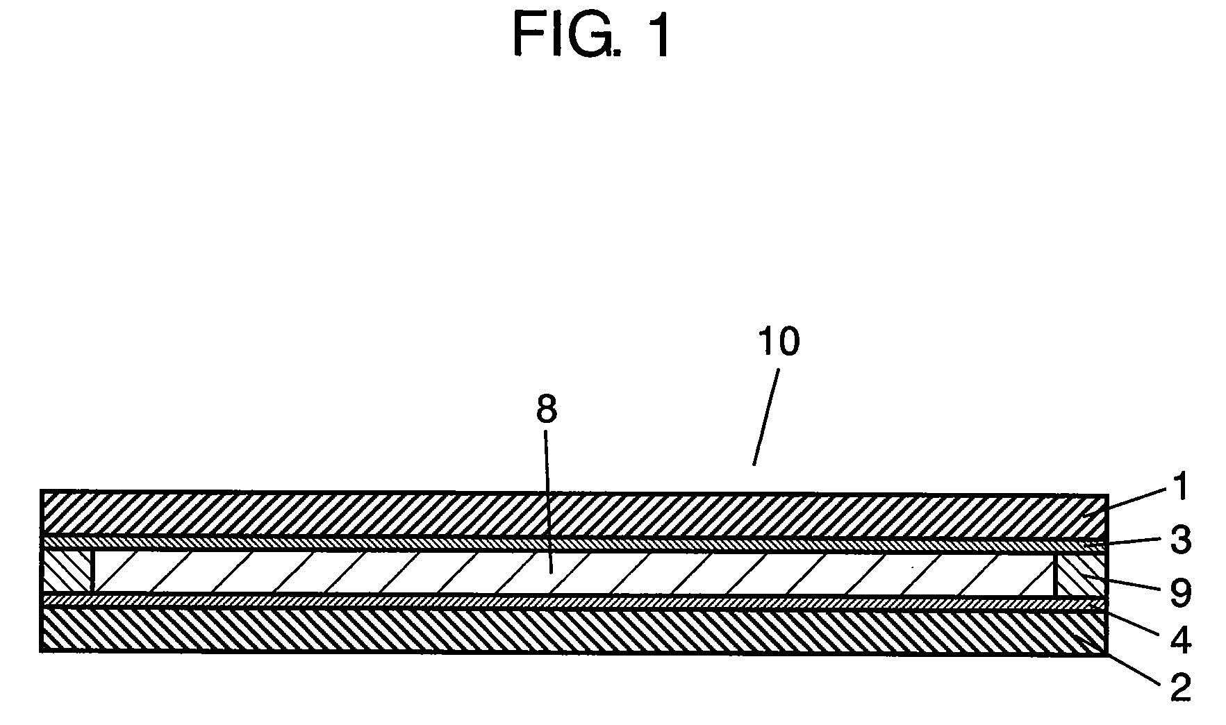
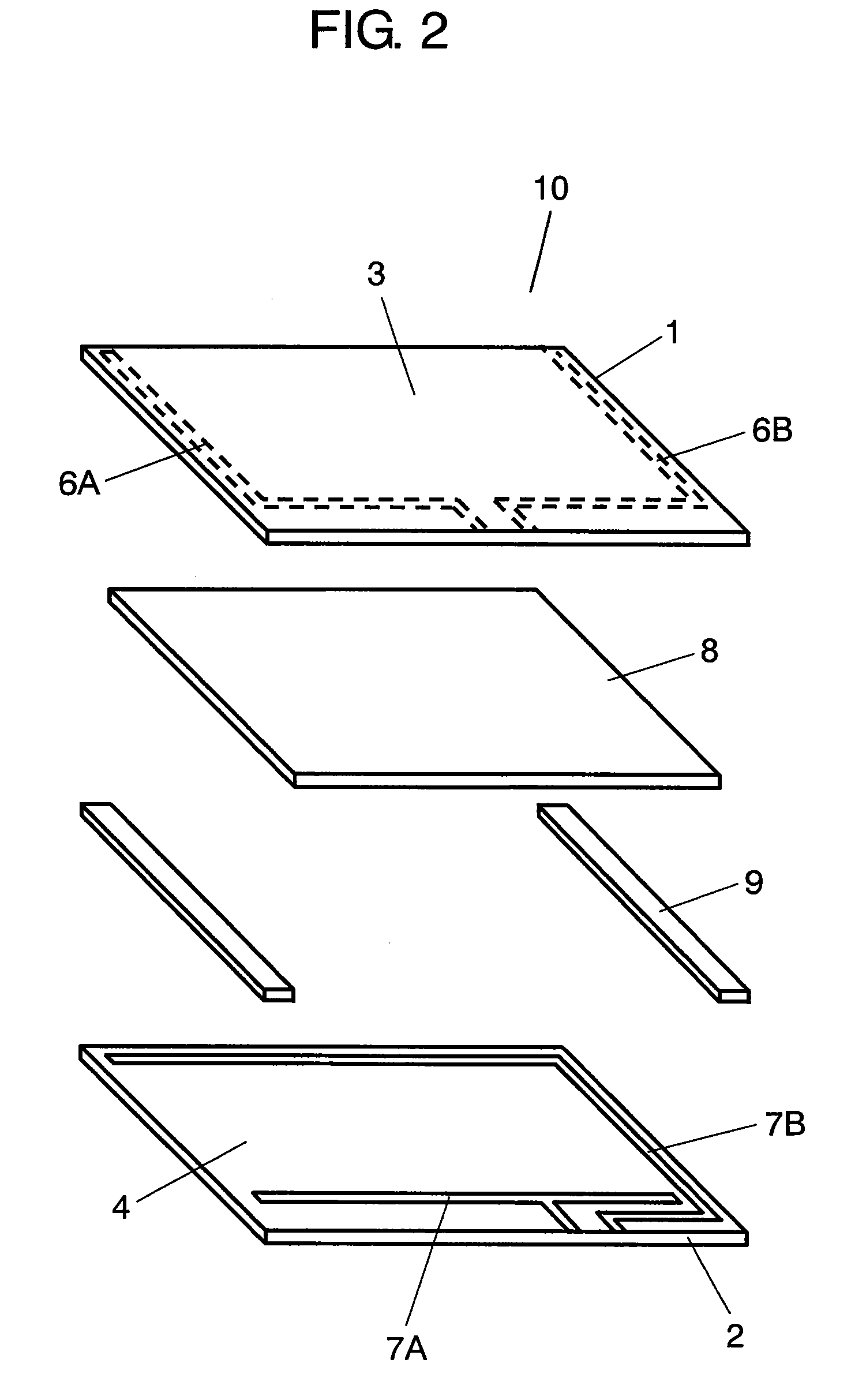
[0023]FIG. 1 is a sectional view and FIG. 2 is an exploded perspective view of a touch panel in an embodiment of the present invention. In FIGS. 1 and 2, touch panel 10 includes light transmitting upper substrate 1, light transmitting lower substrate 2, upper conductive layer 3, lower conductive layer 4, piezoelectric material 8, and adhesive layer 9.

[0024]Light transmitting upper substrate 1 is a light transmitting film made typically of polyethylene terephthalate or polycarbonate. Light transmitting lower substrate 2 is also light transmittable, and is made typically of polycarbonate, glass, or acryl. Light transmitting upper conductive layer 3 made typically of indium tin oxide or tin oxide is formed on a bottom face of light transmitting upper substrate 1, and lower conductive layer 4 is formed on a top face of light transmitting lower substrate 2 in the same way, such as by sputtering.

[0025]A pair of top electrodes 6A and 6B, made typically of silver or carbon, are formed on bo...


PUM

PropertyMeasurementUnit
Thicknessaaaaaaaaaa
Electrical conductoraaaaaaaaaa
Lightaaaaaaaaaa

Abstract

A touch panel that sandwiches a light transmitting piezoelectric material, which generates a voltage by a pressing force, between an upper conductive layer formed on a bottom face of an upper substrate and a lower conductive layer formed on a top face of a lower substrate. Since there is no space between the upper conductive layer and the lower conductive layer, reflection of external light can be reduced. This achieves good viewability. In addition, the touch panel can be easily manufactureable just by sequentially superimposing and attaching components

Description

FIELD OF THE INVENTION [0001]The present invention relates to touch panels for typically operating a range of electronic devices.BACKGROUND OF THE INVENTION [0002]With electronic devices such as mobile phones and car navigation systems becoming increasingly sophisticated and diversified, many products are adopting a light transmitting touch panel on a front face of a display device, typically a liquid crystal display. The user of the electronic device views what is displayed on the display device on a rear face of the touch panel through this touch panel, and presses the touch panel typically with a finger or pen. Increasingly more electronic devices are adopting the touch panel for switching functions. Accordingly, the user demands a touch panel with good viewability and reliable operation.[0003]A conventional touch panel is described next with reference to FIG. 3.[0004]In FIG. 3, dimensions in a thickness direction are enlarged for easier understanding of a structure.[0005]FIG. 3 ...

Claims


Application Information

Patent Timeline
IPC IPC(8): H02N2/18H01L41/22G06F3/041H01H13/00H01H13/712
CPCG06F3/041G06F3/0414Y10T29/42H01L41/45H01L41/113G06F3/045H10N30/30H10N30/098
Inventor MATSUMOTO, KENICHI
Owner PANASONIC INTELLECTUAL PROPERTY MANAGEMENT CO LTD
Why Eureka
Try Eureka