Method of controlling on-die termination of memory devices sharing signal lines

a technology of memory devices and signal lines, applied in the field of semiconductor memory devices, can solve problems such as interference mismatches

Active Publication Date: 2008-02-07
SAMSUNG ELECTRONICS CO LTD
View PDF8 Cites 45 Cited by
  • Summary
  • Abstract
  • Description
  • Claims
  • Application Information

AI Technical Summary

Benefits of technology

[0014]Embodiments of the present invention provide a method of actively controlling the On-Die Termination (ODT) impedances of semiconductor devices connected via transmission lines in a semiconductor system. Embodiments of the invention also provide an ODT control method using mode registers

Problems solved by technology

Thus, an impedance mismatch occurs dur

Method used


Image

  • Method of controlling on-die termination of memory devices sharing signal lines
  • Method of controlling on-die termination of memory devices sharing signal lines
  • Method of controlling on-die termination of memory devices sharing signal lines

Examples


Embodiment Construction

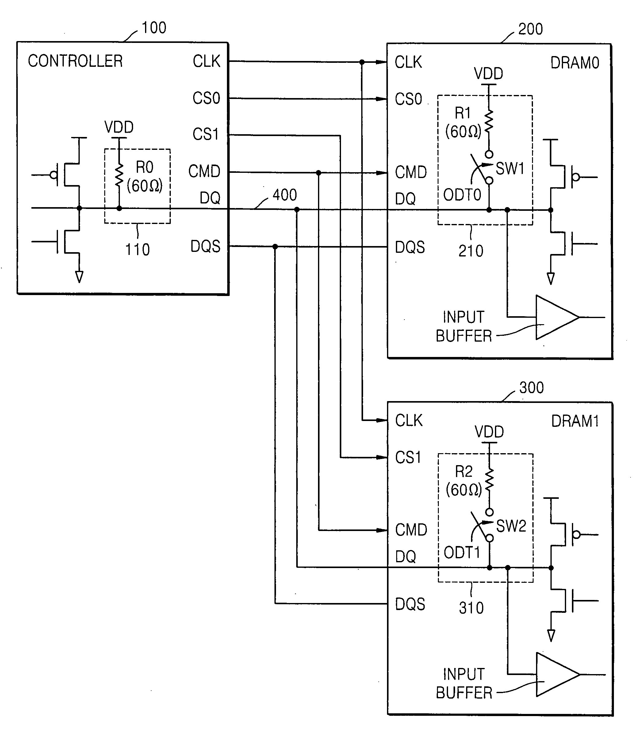
[0025]Embodiments of the invention will now be described more fully with reference to the accompanying drawings. The invention may, however, be embodied in many different forms and should not be construed as being limited to only the embodiments set forth herein. Rather, the embodiments are presented as teaching examples. Throughout the drawings and written description, like reference numerals refer to like or similar elements.

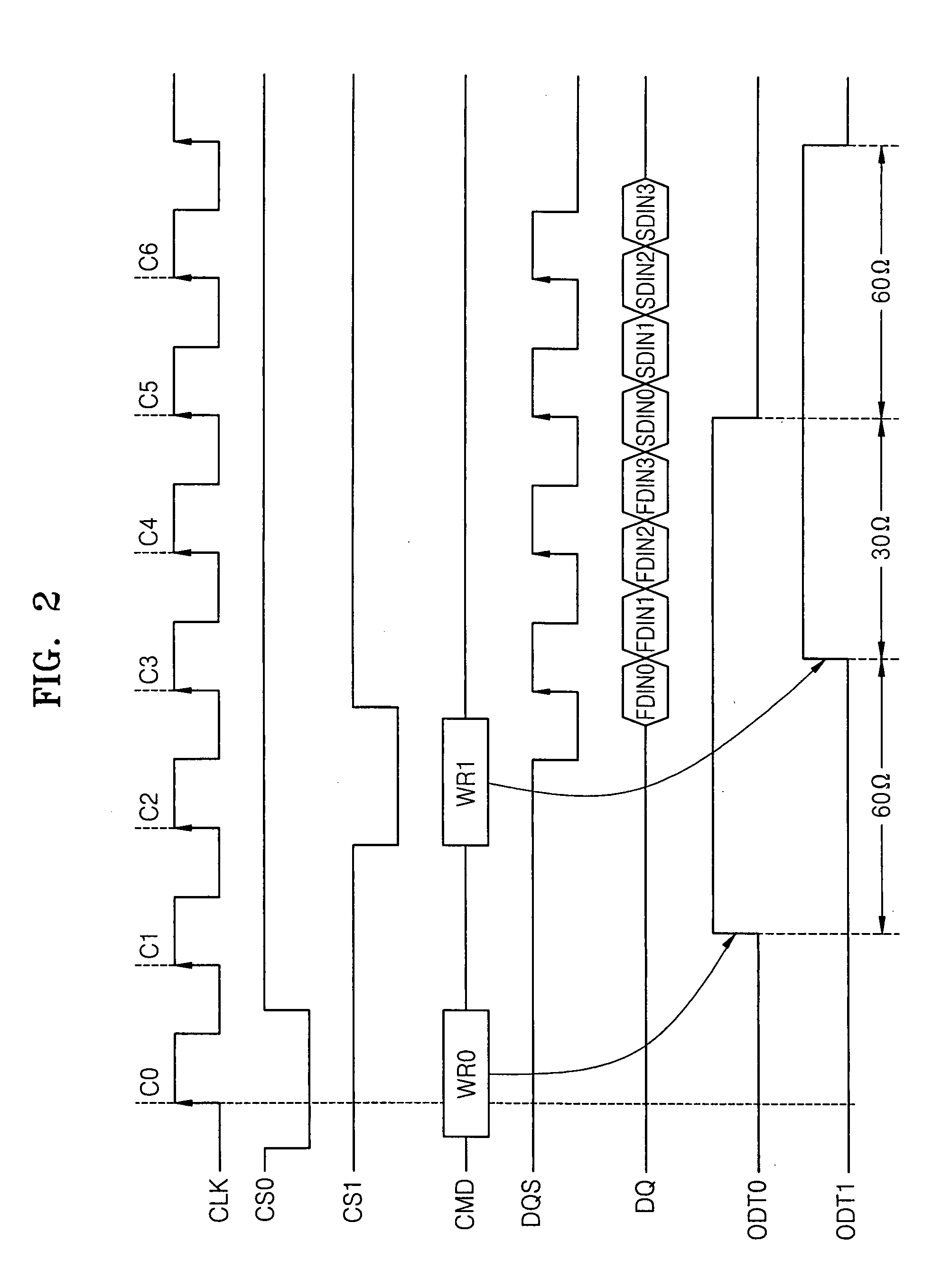
[0026]FIG. 3 is a conceptual diagram illustrating an extended mode register setting method for an On-Die Termination (ODT) control method according to an embodiment of the present invention. Referring to FIG. 3, an extended mode register stores data controlling ODT resistors associated with a semiconductor device, such as a memory device. In the illustrated example, it is assumed that address bits RA1 and RA2 are used to define a data termination state, address bits RA3 and RA4 are used to establish an address and / or command termination state, and address bit ...


PUM


Abstract

A method of controlling On-Die Termination (ODT) resistors of memory devices sharing signal lines is provided. The ODT controlling method comprises setting an ODT control enable signal of each of the memory devices and address/command or data termination information to a mode register of the corresponding memory device, and controlling resistances of ODT resistors of the signal lines in the memory devices in response to the address/command or data termination information and termination addresses. When only one of the memory devices is activated, ODT resistors of the activated memory device are set to a first resistance. When all the memory devices are activated, ODT resistors of the memory devices are set to a second resistance.

Description

BACKGROUND OF THE INVENTION[0001]1. Field of the Invention[0002]The present invention relates to semiconductor devices and systems incorporating same. More particularly, the invention relates to a method of controlling on-die terminations for semiconductor memory devices sharing one or more transmission line (e.g., address lines, command lines, and / or data lines).[0003]This application claims the benefit of Korean Patent Application No. 10-2006-0054370, filed on Jun. 16, 2006, the subject matter of which is hereby incorporated by reference.[0004]2. Description of the Related Art[0005]Within semiconductor systems, it is generally necessary to match the impedance of a transmission line with a corresponding termination impedance (e.g., a resistor) in order to prevent undesirable signal reflections. Such signal reflections act as noise on the signal line in relation to signals subsequently transmitted on the transmission line.[0006]Figure (FIG.) 1 is a block diagram of a conventional se...

Claims


Application Information

Patent Timeline
IPC IPC(8): H03K19/003
CPCH04L25/0278H03K19/0005G11C7/1048G11C7/22
Inventor LEE, DONG-WOOCHOI, JUNG-YONG
Owner SAMSUNG ELECTRONICS CO LTD
Why Eureka
Try Eureka