Devices and methods for controlling active termination resistors in a memory system

a technology of active termination resistor and memory system, which is applied in the field of memory circuits and systems, can solve the problems of degrading signal integrity, increasing data rate, and affecting the operation of memory system

Inactive Publication Date: 2005-03-01
SAMSUNG ELECTRONICS CO LTD
View PDF4 Cites 79 Cited by
  • Summary
  • Abstract
  • Description
  • Claims
  • Application Information

AI Technical Summary

Problems solved by technology

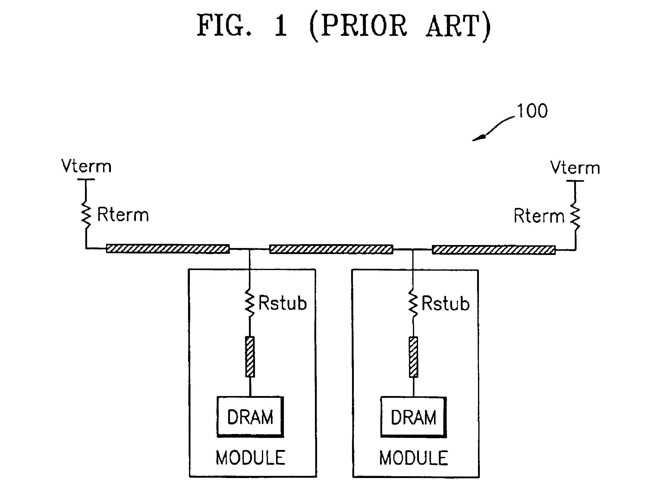
Generally, as the bus frequency of a memory system (e.g., a memory system employing DRAM devices) increases, the signal integrity within the memory system degrades.
However, any increase in data rate beyond 300 Mbps tends to degrade signal integrity by increasing the load of the bus having the resistive stubs.
In fact, a data rate of 400 Mbps or greater is generally not achievable with the SSTL bus configuration.
However, a considerable amount of time is required to enable the active termination resistors installed in the DRAM circuits in response to the active termination control signals, and when a module-interleaved write / read operation is performed, this time lapse can result in data bobbles, thereby degrading memory system performance.
However, in the case where the DLL or PLL is deactivated during a power down or standby mode of a corresponding memory module, enabling / disabling of the active termination resistor cannot be controlled.

Method used


Image

  • Devices and methods for controlling active termination resistors in a memory system
  • Devices and methods for controlling active termination resistors in a memory system
  • Devices and methods for controlling active termination resistors in a memory system

Examples


second embodiment

the present invention will now be described with initial reference to FIG. 11 of the drawings. In this embodiment, DRAM chips positioned on each side of each DiMM module are individually ATC controlled by the combination of common ATC signaling and mode registers. In particular, as shown in FIG. 11, the memory system 1100 includes a chipset 1110, a data bus 1120, a first memory module 1140 in which DRAMs 1160 and 1170 are mounted, and a second memory module 1150 in which DRAMs 1180 and 1190 are mounted. The memory modules 1140 and 1150 may be mounted in card slots (not shown) of the memory system 1100.

The first and second memory modules 1140 and 1150 may be implemented, for example, by a dual in-line memory module (DiMM). Further, while two DRAMs (1160, 1170 and 1180, 1190) are illustrated in FIG. 11 for each of the modules 1140 and 1150, additional DRAMs may be mounted in each of the first and second memory modules 1140 and 1150. Also, each of the chipset 1110 and the DRAMs 1160, 1...

third embodiment

the present invention will now be described with reference to FIG. 17 of the drawings. In this embodiment, DRAM chips positioned on each side of each DiMM module are individually ATC controlled by individual ATC signals issued from the chipset. In particular, as shown in FIG. 17, the memory system 1700 includes a chipset 1710, a data bus 1720, a first memory module 1740 in which DRAMs 1760 and 1770 are mounted, and a second memory module 1750 in which DRAMs 1780 and 1790 are mounted. The memory modules 1740 and 1750 may be mounted in card slots (not shown) of the memory system 1700.

The first and second memory modules 1740 and 1750 may be implemented, for example, by a dual in-line memory module (DiMM). Further, while two DRAMs (1160, 1170 and 1180, 1190) are illustrated in FIG. 17 for each of the modules 1740 and 1750, additional DRAMs may be mounted in each of the first and second memory modules 1740 and 1750. Also, each of the chipset 1710 and the DRAMs 1760, 1770, 1780 and 1790 a...


PUM


Abstract

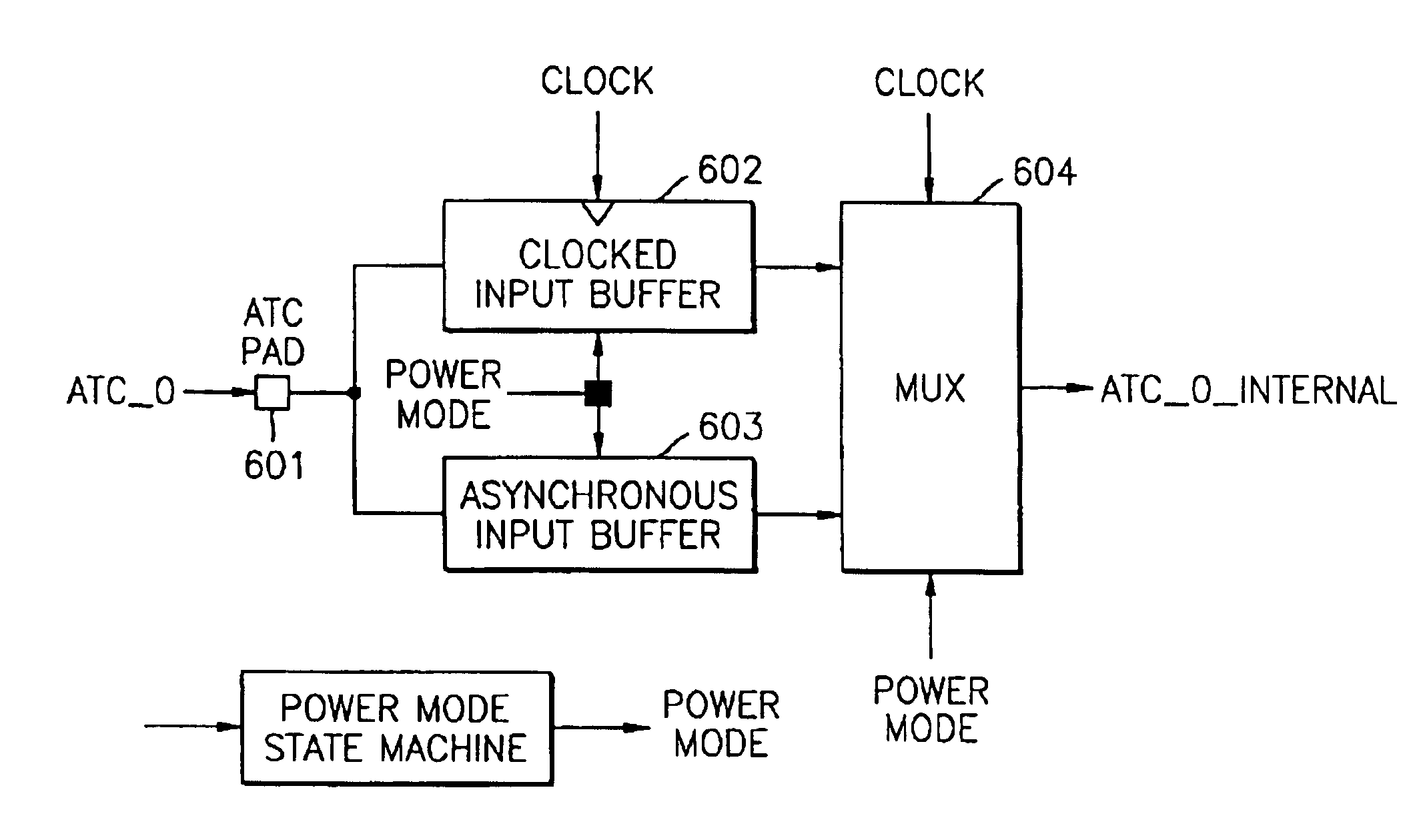
An active termination circuit is mounted in a memory circuit and includes a termination resistor which provides a termination resistance for the memory circuit, and a control circuit which receives an externally supplied active termination control signal, and which selectively switches on and off the termination resistor in response to the active termination control signal. The control circuit includes a synchronous input buffer and an asynchronous input buffer which each receive the active termination control signal, and a switching circuit which selectively outputs an output of said synchronous input buffer or an output of said asynchronous input buffer according to an operational mode of the memory circuit. The output of the switching circuit controls an on / off state of said termination resistor.

Description

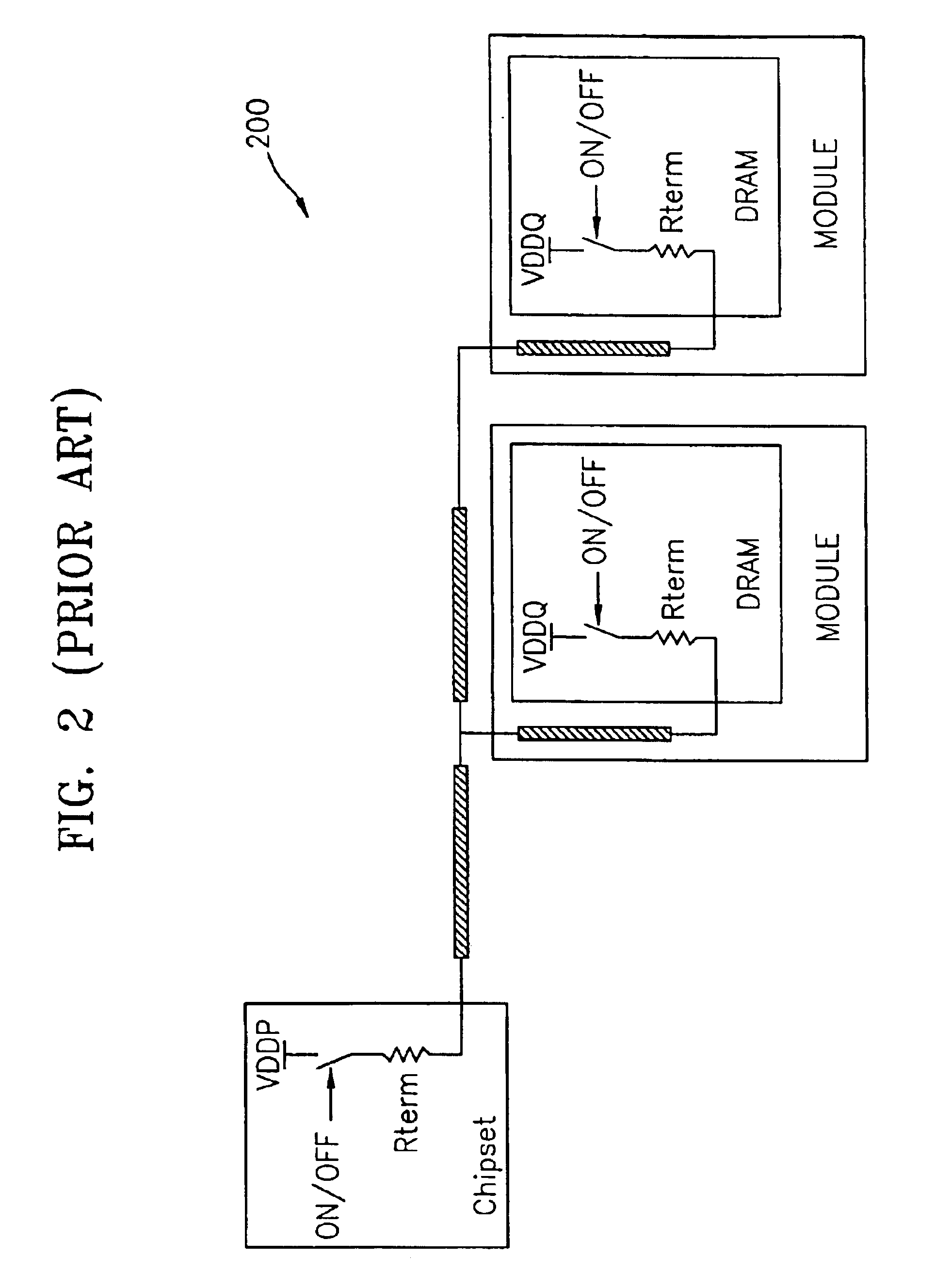
BACKGROUND OF THE INVENTION1. Filed of the InventionThe present invention generally relates to memory circuits and systems, and more particularly, the present invention relates to devices and methods for controlling active termination resistors which are used improve signaling characteristics in memory circuits and systems.2. Description of the Related ArtGenerally, as the bus frequency of a memory system (e.g., a memory system employing DRAM devices) increases, the signal integrity within the memory system degrades. Thus, a variety of bus topologies capable of reducing signal distortion have been developed. For example, it is known that the use of resistive terminations at either the receiver and / or transmitter sides within the memory system is an effective means for absorbing reflections and thereby improving signal performance. Resistive termination configurations of this type generally fall into one of two categories, i.e., passive termination or active termination.FIG. 1 shows ...

Claims


Application Information

Patent Timeline
Patent Type & Authority Patents(United States)
IPC IPC(8): G11C7/00G11C7/10G11C7/22G11C11/4093G11C11/4076G11C11/409G11C11/407
CPCG11C7/1072G11C7/1078G11C7/1084G11C11/4093G11C7/222G11C11/4076G11C7/22
Inventor KYUNG, KYE-HYUN
Owner SAMSUNG ELECTRONICS CO LTD
Why Eureka
Try Eureka