Wireless/Optical Transceiver Devices
a transceiver and optical technology, applied in the direction of electrical equipment, fibre transmission, electromagnetic transmission, etc., can solve the problems of not being commercially available, high cost, and specialised optical devices of afpm
- Summary
- Abstract
- Description
- Claims
- Application Information
AI Technical Summary
Benefits of technology
Problems solved by technology
Method used
Image

Examples
first embodiment
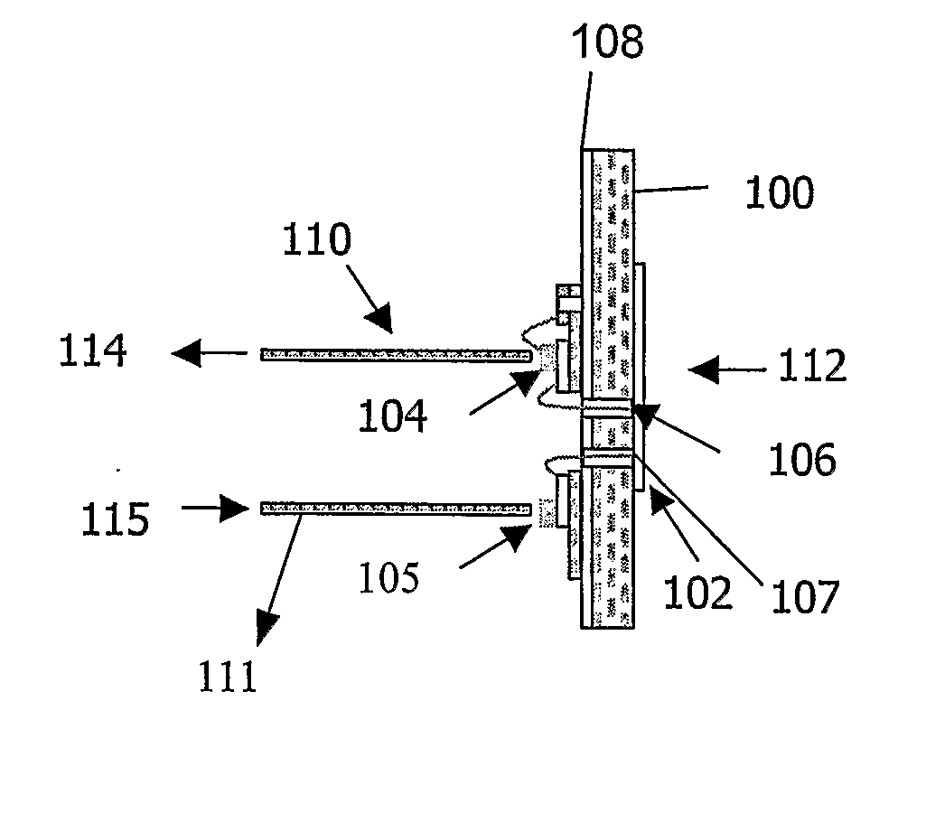
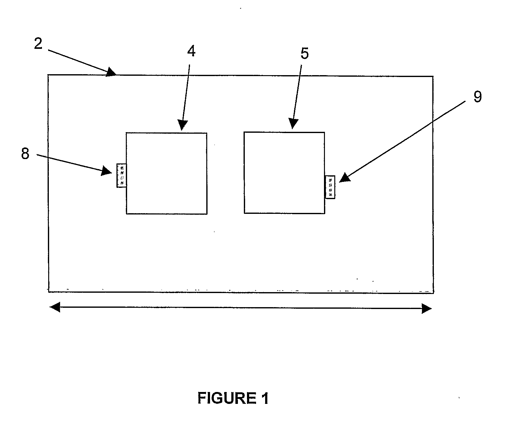
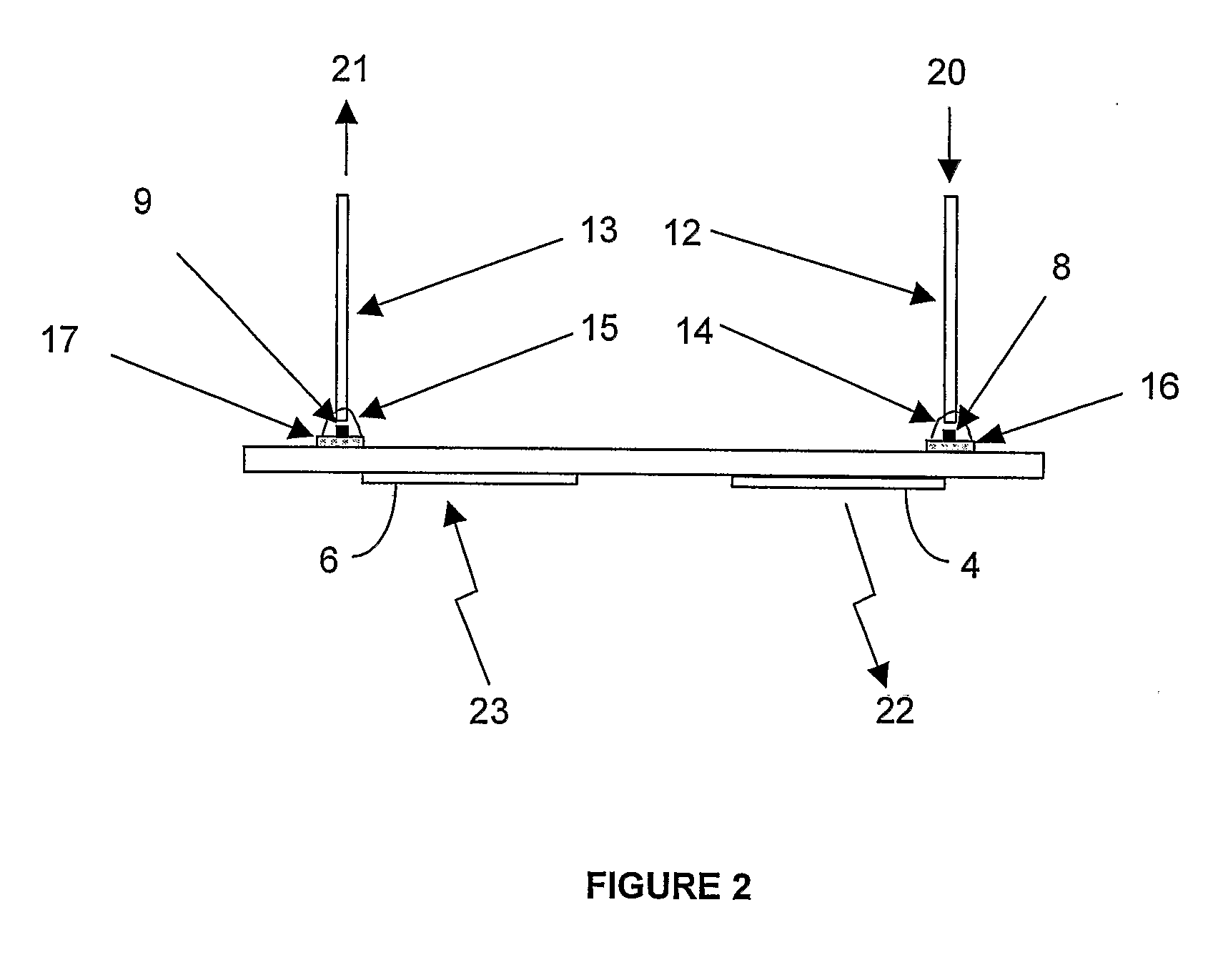
[0021]FIGS. 1 and 2 illustrate, in plan and side views respectively, a first transceiver 1 embodying the present invention. In this first embodiment, a substrate 2 carries a transmit antenna 4 and a receive antenna 5.
[0022] A photodiode (PD) 8 is located adjacent the transmit antenna 4 on the substrate 2, and is electrically connected with the transmit antenna 4. A bias voltage connection of the photodiode 8 is connected with the transmit antenna 4.
[0023] A vertical cavity semiconductor laser (VCSEL) device 9 is provided on the substrate adjacent the receive antenna 5, and is electrically connected with the receive antenna 5. The receive antenna 5 is connected with a bias voltage connection of the VCSEL 9.
[0024] The photodiode 8 and the VCSEL device 9 are supplied with electrical current from a power supply (not shown for the sake of clarity).
[0025] In the example shown in FIGS. 1 and 2, the photodiode 8 and VCSEL device 9 are carried on an opposite side of the substrate to the a...
fifth embodiment
[0041]FIGS. 6 and 7 illustrate the present invention in which a substrate 60 carries an antenna on one side. The antenna comprises a ground plane 61 and a slot ring 62. The ground plane 61 and slot ring 62 form a small scale antenna to which a VCSEL device 63 is connected.
[0042] In this embodiment, the antenna is formed directly on a semiconductor substrate such as InP or GaAs. This enables monolithic fabrication of both the laser device (and photodiode device) and the antenna at the same time which could drastically reduce manufacturing costs.
[0043]FIG. 8 illustrates a monolithic semiconductor laser device which embodies a further aspect of the present invention, and that provides a monolithic photonic active integrated antenna. The embodiment of FIG. 8 comprises a substrate 70 which carries a semiconductor laser device 71. The laser device 71 includes an active region 74 from which an optical signal 75 is emitted when the device is biased correctly with an electrical signal recei...
PUM
 Abstract
Description
Claims
Application Information
 - R&D
- Intellectual Property
- Life Sciences
- Materials
- Tech Scout
- Unparalleled Data Quality
- Higher Quality Content
- 60% Fewer Hallucinations
Browse by: Latest US Patents, China's latest patents, Technical Efficacy Thesaurus, Application Domain, Technology Topic, Popular Technical Reports.
© 2025 PatSnap. All rights reserved.Legal|Privacy policy|Modern Slavery Act Transparency Statement|Sitemap|About US| Contact US: help@patsnap.com