Light emitting device, method of making the same, and light source device comprising the same

a technology light source, which is applied in the manufacture of electrode systems, electric discharge tubes/lamps, transportation and packaging, etc., can solve the problems of reducing excitation efficiency, phosphor also becoming high temperature at glass melting, and deterioration of translucent resin, so as to reduce color heterogeneity of light, reduce the size of light emitting device, and prevent sealing portion from deterioration

Inactive Publication Date: 2008-02-07
TOYODA GOSEI CO LTD
View PDF21 Cites 41 Cited by
  • Summary
  • Abstract
  • Description
  • Claims
  • Application Information

AI Technical Summary

Benefits of technology

[0055] According to the invention, a light emitting device capable of preventing the sealing portion from deteriorating by using glass material for sealing the light emitting device, and simultaneously reducing color the heterogeneity of light obtained can be provided.
[0056] In particular, according to the light emitting device in embodiment (1), the transparent member positioned outside of the glass member, so that the light emitted from the light emitting element is emitted outward after it was transmitted through the transparent member.
[0057] At this time, the phosphor attached to the transparent member emits a wavelength conversion light when excited by the light emitting from the light emitting element. And, when the light emitted from the light emitting element and the wavelength conversion light emitted from the phosphor are combined, white light can be obtained.
[0058] Further, the powdery phosphor adheres to an inner surface, an outer surface or both of the inner surface and outer surface of the transparent member, so that the phosphor can be evenly distributed on the transparent member. Thus, the light emitting device can be reduced in size. And, the thickness of the phosphor does not change at a specific site on the transparent member, so that the light emitted from the light emitting device can be evenly wavelength-converted without dependence on the path of light.
[0059] Further, a trouble that the covering member must be installed individually is eliminated, so that a mass productivity can be enhanced, and decrease in an emission property of the light emitted from the light emitting device is prevented, so that a stable light distribution can be obtained.

Problems solved by technology

These solid state devices have a problem that the translucent resin deteriorates due to a light emitted from the solid state element.
However, in the former case, the sealing by using a glass material requires a higher sealing temperature in comparison with the sealing by using a usual translucent resin member, so that the phosphor also becomes high temperature at the glass melting.
Further, if a crystalline inorganic phosphor is used, excitation efficiency may be remarkably decreased.
In the latter case, the phosphor comprises a higher specific gravity than that of the translucent resin, and the phosphor sinks into the translucent resin before the resin is hardened, so that it is difficult to disperse the phosphor into the translucent resin homogeneously, and color heterogeneity easily occurs.
Further, in the light emitting device described in Patent Literature 2, there is a problem that the covering member including the phosphor comprises an even thickness, so that the light emitting device must be increased in size.
And, there is a problem that with dependence on the path of light emitted from the light emitting element, difference of light path length from the incoming position to the outgoing position of the covering member occurs, so that the color heterogeneity of light being wavelength-converted by the covering member also occurs.
Further, there is a problem that the installation of the covering member including the phosphor in the glass sealed LED takes a lot of trouble, and simultaneously the light taking out efficiency is reduced due to air interfusion between the glass sealed LED and the covering member, and unevenness of light distribution occurs.

Method used


Image

  • Light emitting device, method of making the same, and light source device comprising the same
  • Light emitting device, method of making the same, and light source device comprising the same
  • Light emitting device, method of making the same, and light source device comprising the same

Examples


Embodiment Construction

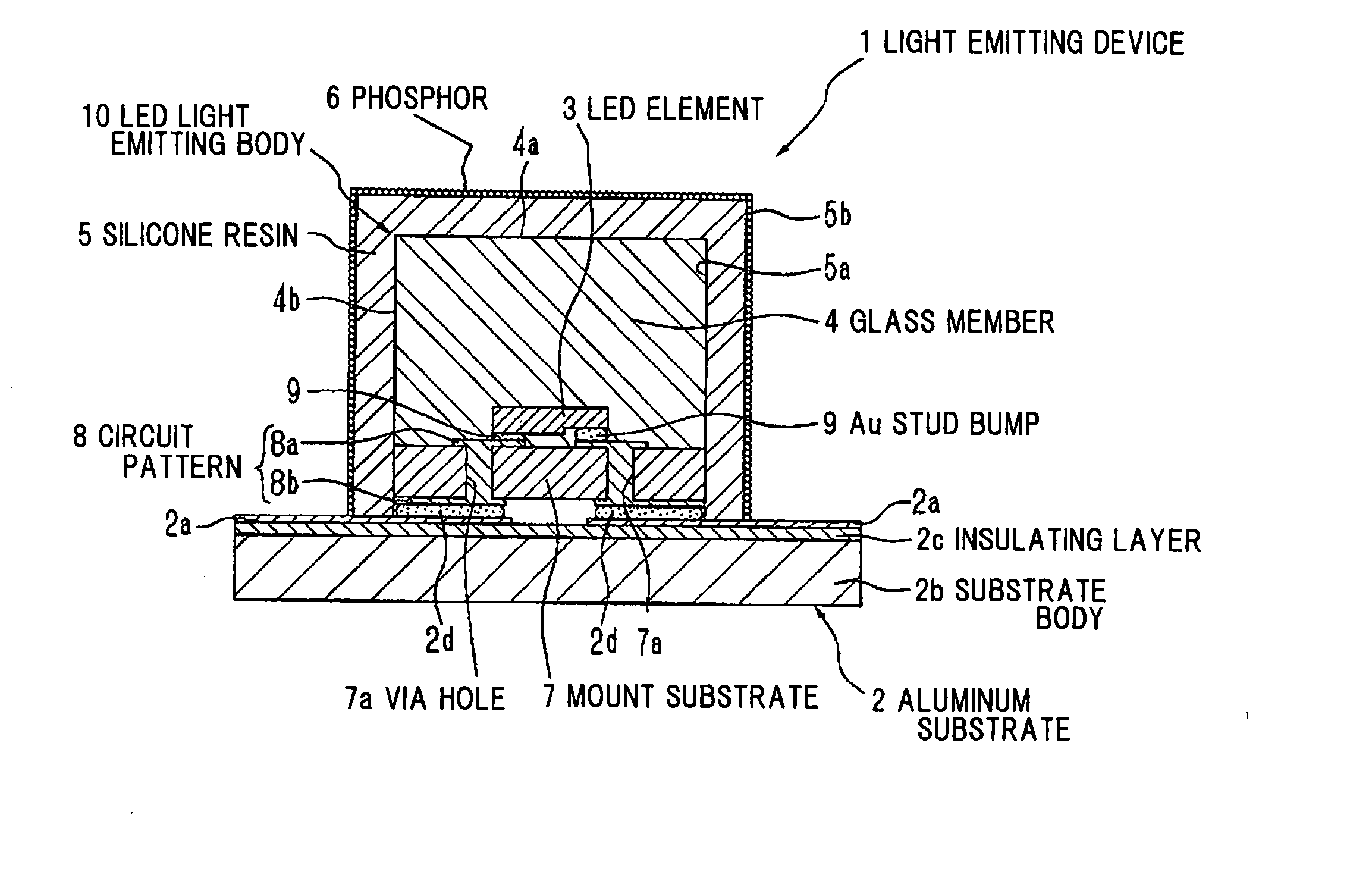
[0079] FIGS. 1 to 4 shows a first preferred embodiment according to the invention, and FIG. 1 is a cross sectional view schematically showing a light emitting device.

[0080] As shown in FIG. 1, a light emitting device 1 comprises a LED element 3 as a light emitting element mounted on an aluminum base substrate 2 (hereinafter referred to as “aluminum substrate 2”), a glass member 4 sealing the LED element 3, a transparent silicone resin 5 surrounding the opposite side of the LED element 3 to the aluminum substrate 2, and a powdery phosphor 6 overall attached to the opposite surface to the aluminum substrate 2 (outer surface 5b) of the silicone resin 5.

[0081] The aluminum substrate 2 comprises a substrate body 2b comprising aluminum, and an insulating layer 2c formed on the substrate body 2b. On the insulating layer 2c constituting a mounting surface of the aluminum substrate 2, a wiring portion 2a to supply an electrical power to the LED element 3 is formed. The wiring portion 2a co...


PUM

PropertyMeasurementUnit
temperatureaaaaaaaaaa
sizeaaaaaaaaaa

Abstract

A light emitting device has a light emitting element mounted on a substrate, a glass member sealing the light emitting element, a transparent member to transmit light emitted from the light emitting device, the transparent member being positioned outside the glass member, and a powdery phosphor attached to an inner surface, an outer surface or both of the inner surface and outer surface of the transparent member.

Description

[0001] The present application is based on Japanese patent application No. 2006-212631 and No. 2007-172383, the entire contents of which are incorporated herein by reference. BACKGROUND OF THE INVENTION [0002] 1. Field of the Invention [0003] This invention relates to a light emitting device and, in particular, to a light emitting device in which a light emitting element on a substrate is sealed with a glass member. Also, this invention relates to a method of making the same and a light source device comprising the same. [0004] 2. Description of the Related Art [0005] Conventionally, solid state devices in which a solid state element such as Light Emitting Diode (LED) is sealed with a translucent resin member such as epoxy resin are known. These solid state devices have a problem that the translucent resin deteriorates due to a light emitted from the solid state element. In particular, when III group nitride compound semiconductor light emitting element to emit a light of short wave...

Claims


Application Information

Patent Timeline
Patent Type & Authority Applications(United States)
IPC IPC(8): B32B9/04C09K11/70H01L33/32H01L33/50H01L33/54H01L33/56H01L33/60H01L33/62
CPCH01L33/507H01L2224/13H01L33/56H01L33/54H01L2224/0554H01L2224/05568H01L2224/05573H01L2924/00014Y10T428/31663H01L2224/05599H01L2224/0555H01L2224/0556
Inventor TASUMI, KOJISUEHIRO, YOSHINOBUYAMAGUCHI, SEIJI
Owner TOYODA GOSEI CO LTD
Why Eureka
Try Eureka