Fabricating Zinc oxide semiconductor using hydrolysis

Active Publication Date: 2008-02-07
XEROX CORP
View PDF5 Cites 45 Cited by
  • Summary
  • Abstract
  • Description
  • Claims
  • Application Information

AI Technical Summary

Benefits of technology

[0010]wherein the activities (a), (b), and (c) are each accomplished a number of times in any ef

Problems solved by technology

Conventional fabrication processes for a zinc oxide semiconductor layer for TFTs ma

Method used


Image

  • Fabricating Zinc oxide semiconductor using hydrolysis
  • Fabricating Zinc oxide semiconductor using hydrolysis
  • Fabricating Zinc oxide semiconductor using hydrolysis

Examples


Example

EXAMPLE

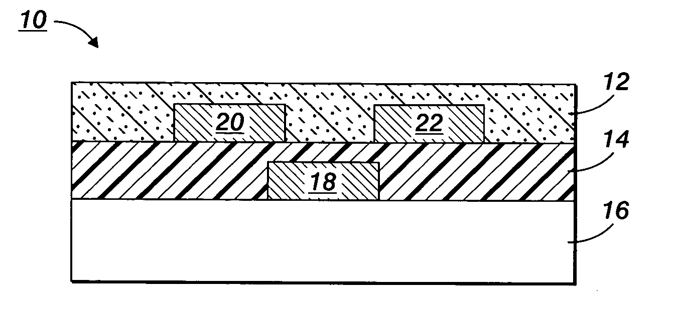
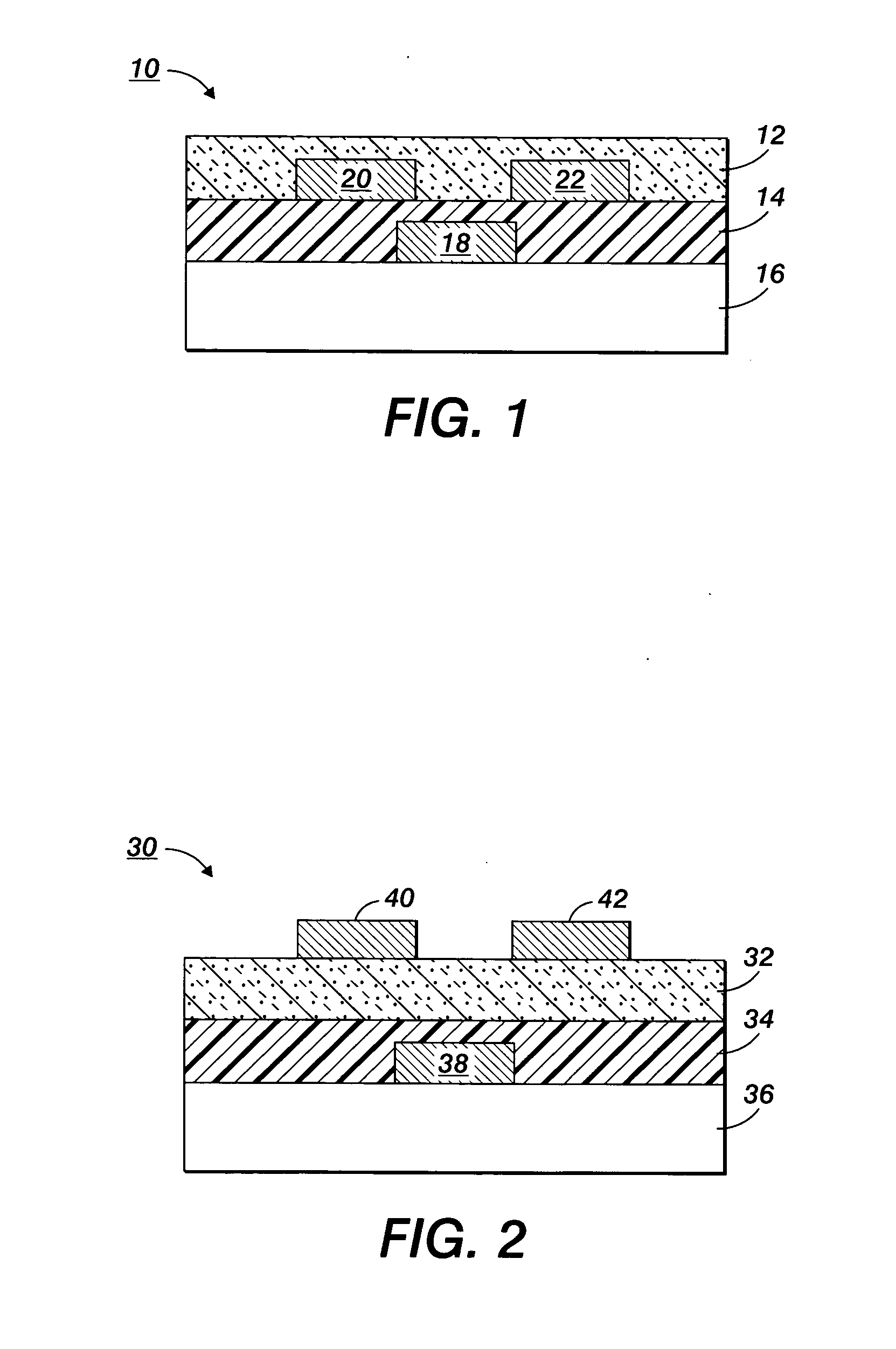
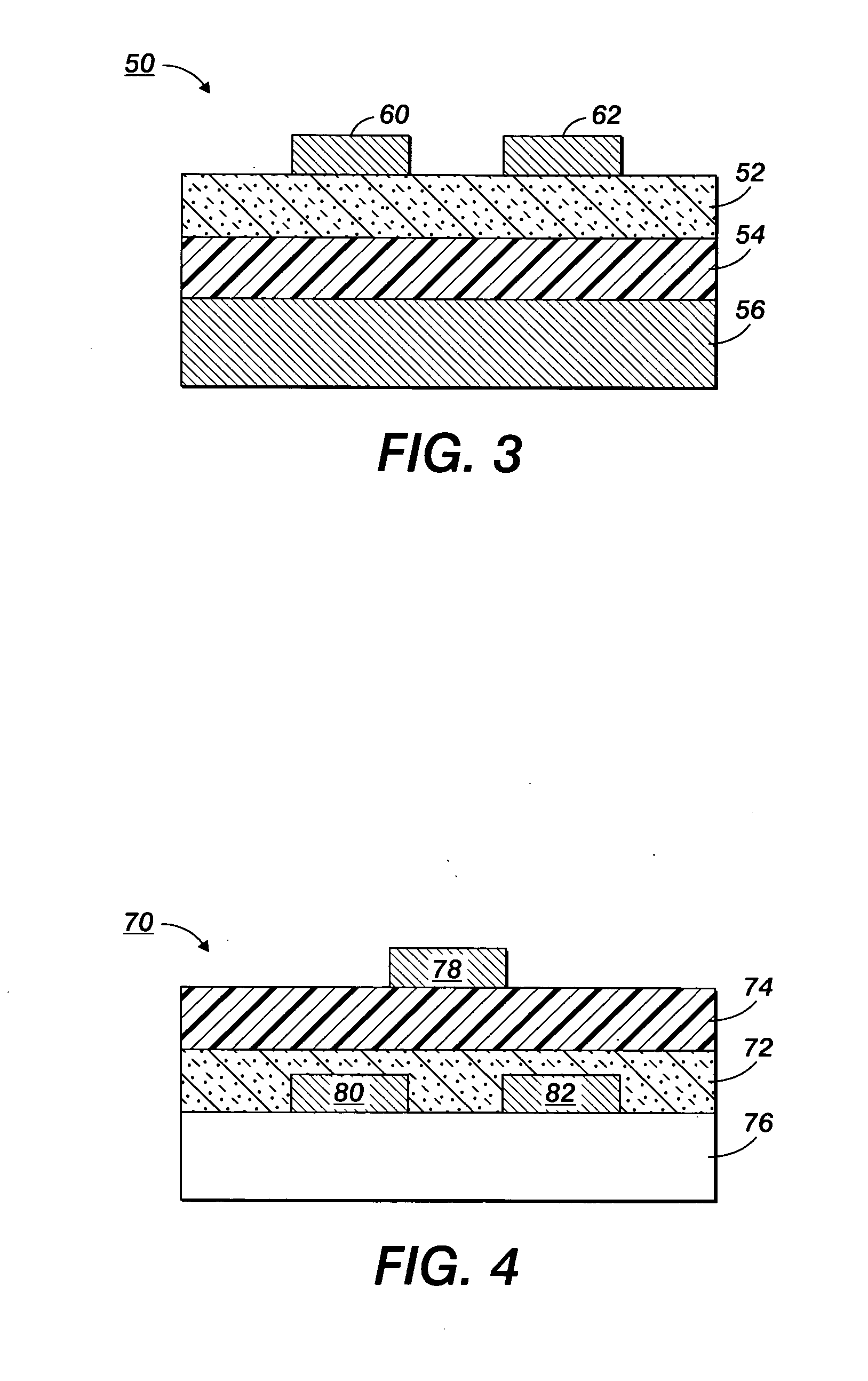
[0063]A TFT device having the configuration of FIG. 3 was prepared as follows. Diethylzinc (1.1M in toluene, Aldrich) was used as precursor to form the ZnO layer. The solution was first diluted with THF to 0.5 M, then spin coated onto n-doped silicon wafer which has 200 nm silicon oxide as dielectric layer. The resulting film was first aged at room temperature at a relative humidity about 40% for 24 hours to hydrolyze the zinc oxide precursor, then annealed at 110 degree C. for 30 min. Al electrodes were vacuum-deposited on top of the ZnO layer to form a series of transistors with different channel length and width. The devices were evaluated using Keithley 4200 SCS System. The saturated carrier mobility, μ, was calculated according to equation (1)

ISD=Ciμ(W / 2L) (VG−VT)2   (1)

where ISD=drain current at the saturated regime, W and L are respectively channel width and length, Ci is the capacitance per unit area of the gate dielectric layer, and VG and VT are respectively gate vo...


PUM


Abstract

A process for fabricating at least one semiconductor layer of an electronic device including: performing on a composition including a hydrolyzable zinc compound a number of activities including: (a) hydrolyzing at least a portion of the hydrolyzable zinc compound to form zinc oxide; (b) liquid depositing; and (c) optionally heating, wherein the activities (a), (b), and (c) are each accomplished a number of times in any effective arrangement, resulting in the at least one semiconductor layer comprising the zinc oxide.

Description

BACKGROUND OF THE INVENTION[0001]Zinc oxide is a promising channel semiconductor in thin film transistors (“TFTs”) for fabricating low cost TFT circuits for large area displays and other low cost electronics. Conventional fabrication processes for a zinc oxide semiconductor layer for TFTs may be costly, involving high equipment investment and complex processing techniques. Thus, there is a need addressed by embodiments of the present invention for simpler, less costly fabrication processes, preferably at a plastic substrate compatible temperature, for a zinc oxide semiconductor layer for electronic devices.[0002]The following documents provide background information:[0003]E. Fortunato et al., “Fully Transparent ZnO Thin-Film Transistor Produced at Room Temperature,”Adv. Mater., Vol. 17, No. 5, pp. 590-594 (Mar. 8, 2005).[0004]B. J. Norris et al., “Spin coated zinc oxide transparent transistors,”J. Phys. D: Appl. Phys., Vol. 36, pp. L105-L107 (2003).[0005]B. Sun et al., “Solution-Pro...

Claims


Application Information

Patent Timeline
IPC IPC(8): H01L21/84H01L21/00
CPCH01L29/7869
Inventor WU, YILIANGONG, BENG S.
Owner XEROX CORP
Why Eureka
Try Eureka