

Thin-film transistor, method of producing the same, and devices provided with the same
a thin-film transistor and film technology, applied in the direction of transistors, semiconductor devices, electrical equipment, etc., can solve the problems of high process temperature of film transistors, inability to provide large-area flexible thin-film transistors at low cost, and inability to meet the requirements of high-definition display applications, etc., to achieve the effect of increasing the carrier density, increasing the oxygen deficiency, and decreasing the mobility
- Summary
- Abstract
- Description
- Claims
- Application Information
AI Technical Summary
Benefits of technology
Problems solved by technology
Method used
Image

Examples
example 1
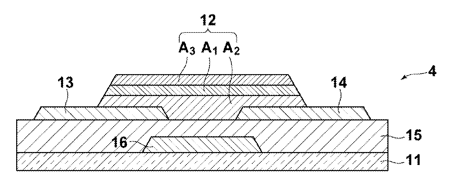
[0217]A top-gate top-contact thin-film transistor having the structure shown at “A” in FIG. 3 was produced as Example 1.
[0218]As the substrate 11, a synthetic quartz glass substrate (T-4040, available from Covalent Materials Corporation) was used. The oxide semiconductor layer 12 was made of InGaZnO, which was formed by the following process. First, a 100 nm-thick InGaZnO film, in which Ga / (In+Ga)=0.75 and Zn / (In+Ga)=0.5, was formed through sputtering as the third area A3. Then, a 10 nm-thick IGZO film, in which Ga / (In+Ga)=0.25 and Zn / (In+Ga)=0.5, was formed through sputtering as the first area A1. Further, a 10 nm-thick IGZO film, in which Ga / (In+Ga)=0.75 and Zn / (In+Ga)=0.5, was formed through sputtering as the second area A2. The film formation of the oxide semiconductor layer 12 was continuously carried out without exposing the areas to the atmosphere. The sputtering of each area was achieved through co-sputtering using an In2O3 target, a Ga2O3 target and a ZnO target. Control of...
PUM
 Abstract
Description
Claims
Application Information