

Thin film transistor, display device, and electronic device
- Summary
- Abstract
- Description
- Claims
- Application Information
AI Technical Summary
Benefits of technology
Problems solved by technology
Method used
Image

Examples
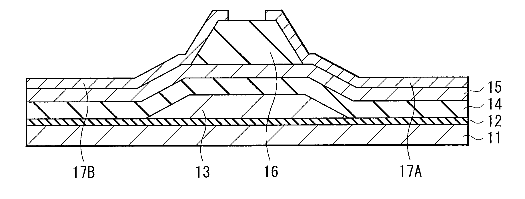
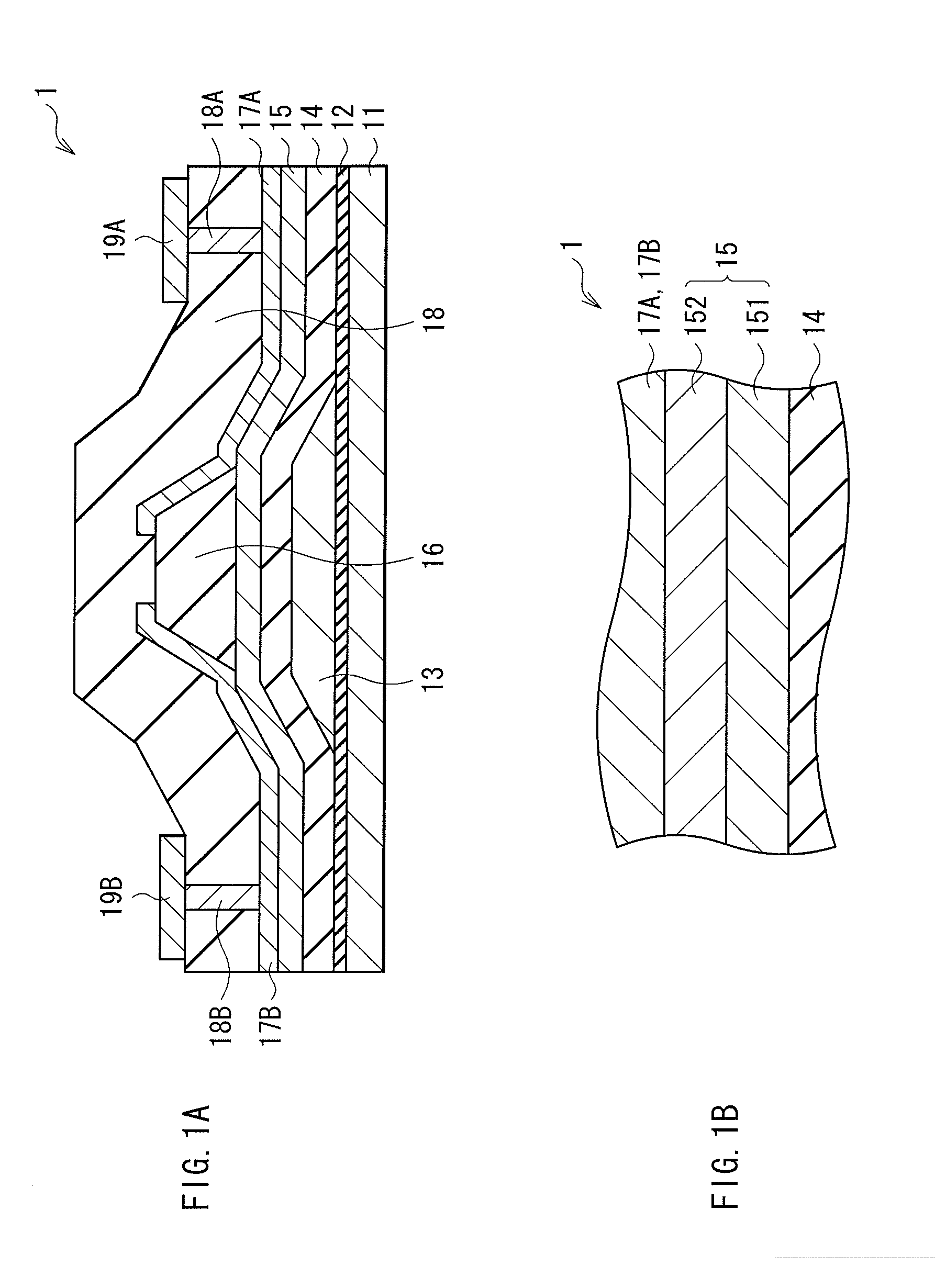
first embodiment
2. Modifications of First Embodiment
[0105]Next, modifications (modifications 1 to 3) of the first embodiment will be described. The same components as in the first embodiment are marked with the same reference numerals or signs, and description of them is appropriately omitted.
[0106]Modification 1
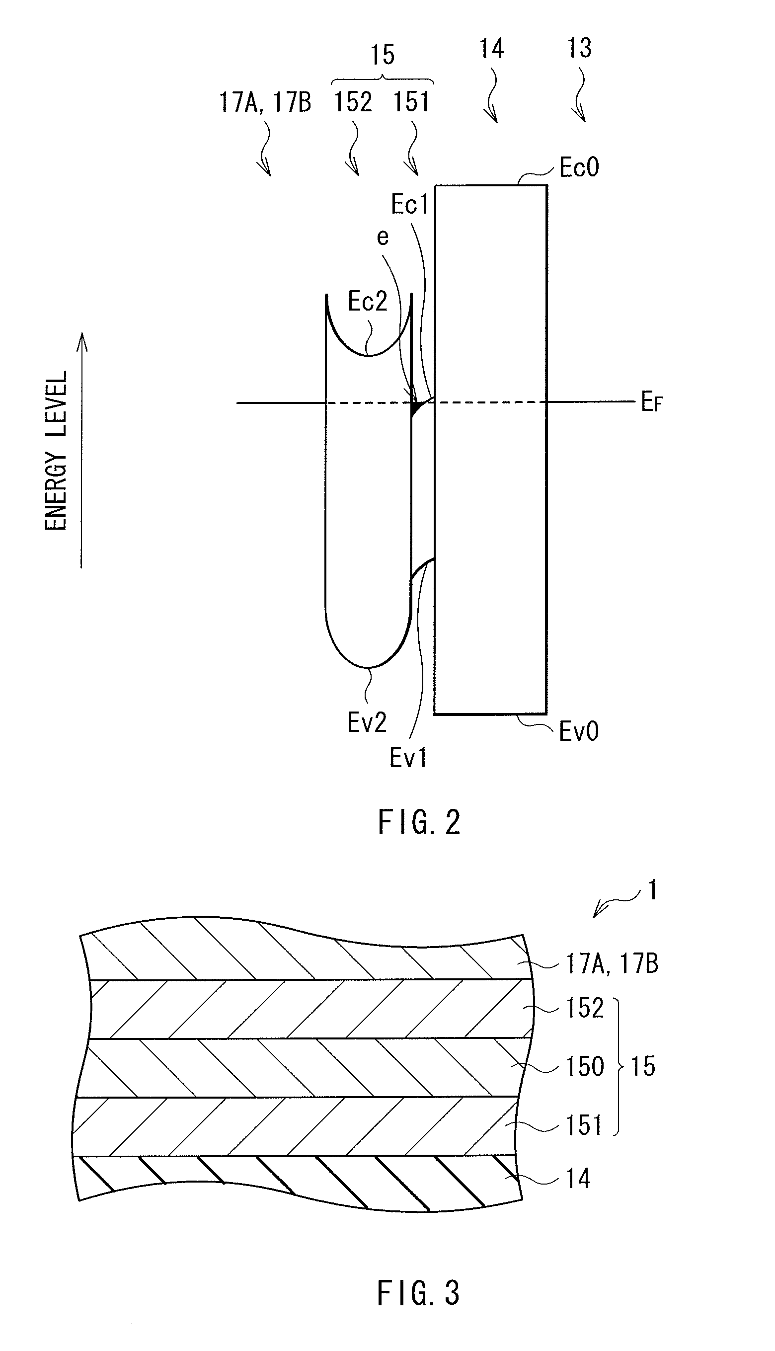
[0107]FIG. 11A shows a sectional configuration of an oxide semiconductor layer 15A of a thin film transistor (TFT 1A) according to modification 1, and FIG. 11B shows an example of an energy band structure of a layer structure around the oxide semiconductor layer 15A.
[0108]As shown in FIGS. 11A and 11B, the TFT 1A of the modification corresponds to TFT having the same configuration as that of the TFT 1 of the first embodiment except that a stacking order of the carrier travel layer 151 and the carrier supply layer 152 in the oxide semiconductor layer 15 is reversed. That is, the oxide semiconductor layer 15A of the modification is configured of a multilayer film (two-layer structure) includi...
second embodiment
4. Modifications of Second Embodiment
[0134]Next, modifications (modifications 4 to 6) of the second embodiment will be described. The same components as in the second embodiment are marked with the same reference numerals or signs, and description of them is appropriately omitted.
[0135]Modification 4
[0136]FIG. 15A shows a sectional configuration of an oxide semiconductor layer 15E of a thin film transistor (TFT 1E) according to modification 4, and FIG. 15B shows an example of an energy band structure of a layer structure around the oxide semiconductor layer 15E.
[0137]As shown in FIGS. 15A and 15B, the TFT 1E of the modification has an oxide semiconductor layer (the oxide semiconductor layer 15E) using a double heterostructure like the TFT 1D of the second embodiment. That is, TFT 1E corresponds to TFT having the same configuration as that of the TFT 1D except that the oxide semiconductor layer 15E is provided in place of the oxide semiconductor layer 15D.
[0138]However, the oxide sem...
application example
[0166]FIG. 19 shows a configuration example of a display device used as an organic EL display (display device 3 including organic EL elements). For example, the display device 3 has a display region 30, in which a plurality of pixels PXLC including organic EL elements (organic field emission elements) as display elements are arranged in a matrix, on a TFT substrate (the substrate 11). A horizontal selector (HSEL) 31 as a signal line drive circuit, a write scanner (WSCN) 32 as a scan line drive circuit, and a drive scanner (DSCN) 33 as a power line drive circuit are provided in the periphery of the display region 30.
[0167]In the display region 30, a plurality of (a whole number n) signal lines DTL1 to DTLn are arranged in a column direction, and a plurality of (a whole number m) scan lines WSL1 to WSLm and a plurality of (a whole number m) power lines DSL1 to DSLm are arranged in a row direction, respectively. Each pixel PXLC (one of pixels corresponding to red (R), ...
PUM
 Abstract
Description
Claims
Application Information