Oxide semiconductor film and semiconductor device

a technology of semiconductor devices and oxide semiconductor films, which is applied in semiconductor devices, electric lighting sources, and electric light sources. it can solve the problems of reducing the electrical conductivity of the oxide semiconductor film might change, and the so as to achieve stable electric conductivity, high reliability of the semiconductor device, and more electrical stability

Active Publication Date: 2012-06-07
SEMICON ENERGY LAB CO LTD
View PDF2 Cites 440 Cited by
  • Summary
  • Abstract
  • Description
  • Claims
  • Application Information

AI Technical Summary

Benefits of technology

[0020]An oxide semiconductor film including a crystalline region in which an a-b plane is substantially parallel with a surface of the film and a c-axis is substantially perpendicular to the surface of the film has stable electric conductivity and is more

Problems solved by technology

However, the electric conductivity of an oxide semiconductor film might change when, for example, a defect typified by an oxygen defect is generated in the oxide semiconductor film, or hydrogen which is to be a source for supplying a carrier enters the oxide semiconductor film in a manufacturing process of the oxide semiconductor film and a semiconductor device including the oxide se

Method used


Image

  • Oxide semiconductor film and semiconductor device
  • Oxide semiconductor film and semiconductor device
  • Oxide semiconductor film and semiconductor device

Examples


embodiment 1

[0055]In this embodiment, an oxide semiconductor film will be described as an embodiment of the present invention with reference to FIG. 1, FIG. 2, FIG. 3, FIG. 4, and FIGS. 5A and 5B.

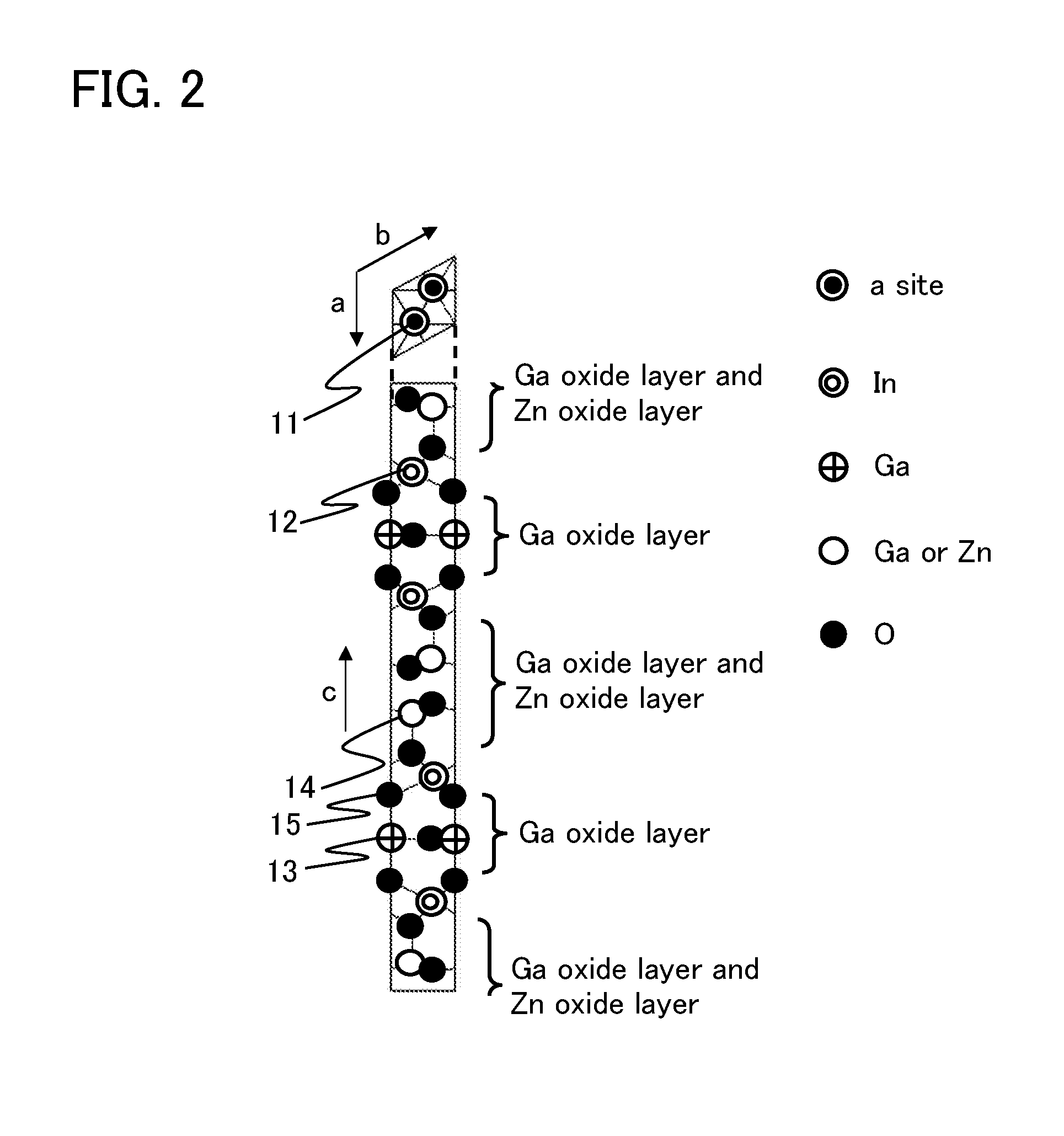
[0056]An oxide semiconductor film according to this embodiment includes a crystalline region. The crystalline region includes a crystal in which an a-b plane is substantially parallel with a surface of the film and a c-axis is substantially perpendicular to the surface of the film. That is, the crystalline region included in the oxide semiconductor film has c-axis alignment. When a cross section of the crystalline region is observed, atoms arranged in a layered manner and stacked from a substrate toward the surface of the film are observed, and the c-axis of the crystal is substantially perpendicular to the surface. Since the oxide semiconductor film includes the crystalline region with c-axis alignment as described above, the oxide semiconductor film is also referred to as a c-axis aligned crystalline...

embodiment 2

[0091]In this embodiment, a transistor in which the oxide semiconductor film including a crystalline region described in Embodiment 1 is used and a method for manufacturing the transistor will be described with reference to FIGS. 6A to 6E, FIGS. 7A and 7B, FIGS. 8A and 8B, FIGS. 9A and 9B, and FIGS. 10A to 10C. FIGS. 6A to 6E are cross-sectional views illustrating a manufacturing process of a top-gate transistor 120 which is an embodiment of the structure of a semiconductor device.

[0092]First, before an oxide semiconductor film including a crystalline region is formed, a base insulating film 53 is preferably formed over a substrate 51 as illustrated in FIG. 6A.

[0093]The substrate 51 should have at least heat resistance high enough to withstand heat treatment performed later. When a glass substrate is used as the substrate 51, a glass substrate whose strain point is higher than or equal to 730° C. is preferably used. As a glass substrate, a substrate formed of a glass material such a...

embodiment 3

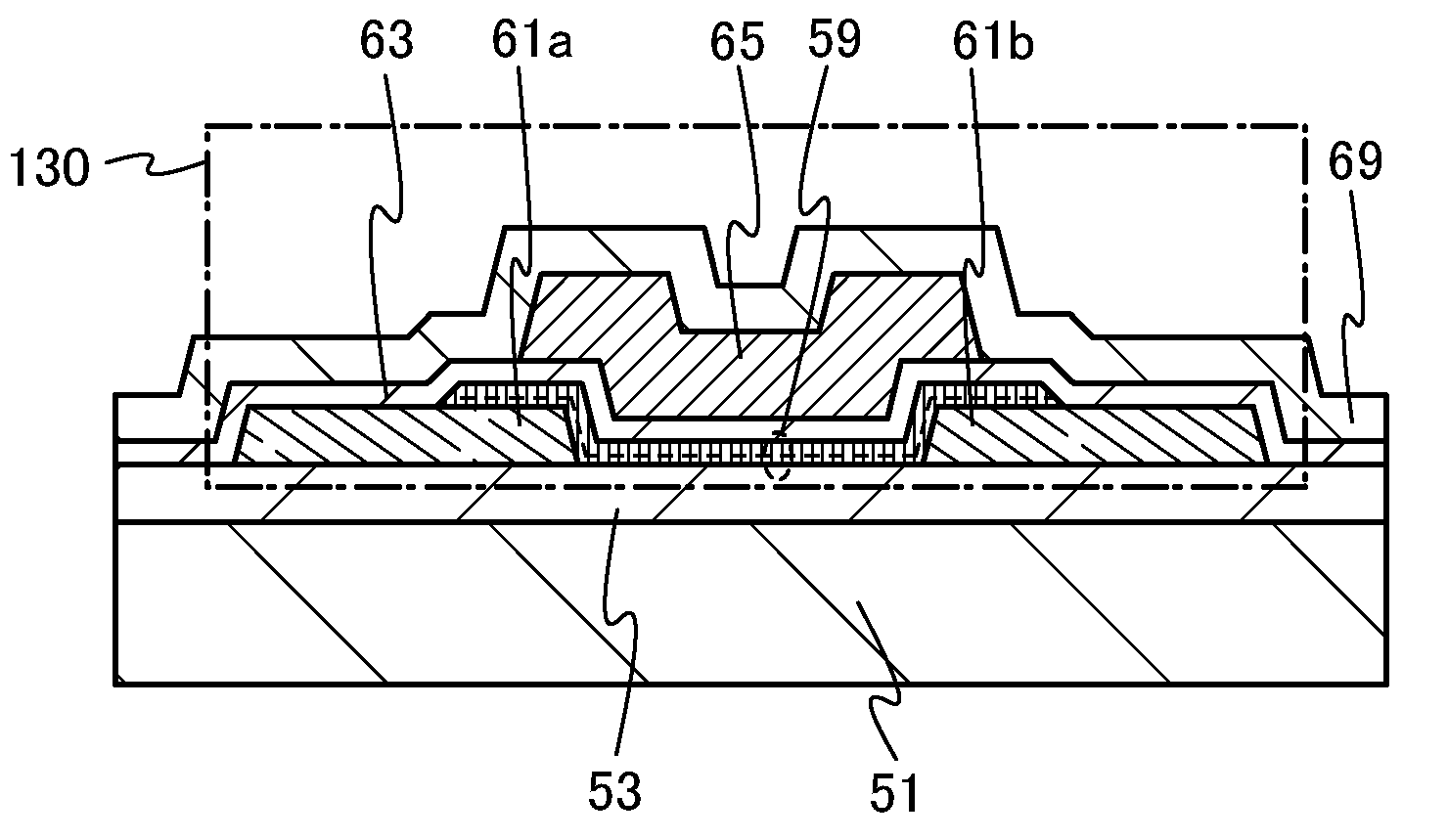
[0168]In this embodiment, a transistor having a structure that is different from that of the transistor which includes the oxide semiconductor film including a crystalline region described in the above embodiment will be described with reference to FIGS. 11A to 11C and FIG. 12.

[0169]A transistor 160 having a top gate structure illustrated in FIG. 11A includes a base insulating film 353 provided over a substrate 351, a metal oxide film 371 provided over the base insulating film 353, an oxide semiconductor film 359 provided over the metal oxide film 371, a source electrode 361a and a drain electrode 361b provided in contact with an upper surface and side surfaces of the oxide semiconductor film 359, a metal oxide film 373 provided over the oxide semiconductor film 359, a gate insulating film 363 provided over the metal oxide film 373, a gate electrode 365 provided over the gate insulating film 363 so as to overlap with the oxide semiconductor film 359, and an insulating film 369 provi...


PUM


Abstract

An oxide semiconductor film which has more stable electric conductivity is provided. Further, a semiconductor device which has stable electric characteristics and high reliability is provided by using the oxide semiconductor film. An oxide semiconductor film includes a crystalline region, and the crystalline region includes a crystal in which an a-b plane is substantially parallel with a surface of the film and a c-axis is substantially perpendicular to the surface of the film; the oxide semiconductor film has stable electric conductivity and is more electrically stable with respect to irradiation with visible light, ultraviolet light, and the like. By using such an oxide semiconductor film for a transistor, a highly reliable semiconductor device having stable electric characteristics can be provided.

Description

TECHNICAL FIELD[0001]An embodiment of the present invention relates to an oxide semiconductor film and a semiconductor device including the oxide semiconductor film.[0002]In this specification, a semiconductor device refers to any device that can function by utilizing semiconductor characteristics, and electro-optical devices, semiconductor circuits, and electronic devices are all semiconductor devices.BACKGROUND ART[0003]As typically seen in a liquid crystal display device, a transistor formed over a glass substrate or the like is manufactured using amorphous silicon, polycrystalline silicon, or the like. A transistor manufactured using amorphous silicon can easily be formed over a larger glass substrate. However, a transistor manufactured using amorphous silicon has a disadvantage of low field-effect mobility. Although a transistor manufactured using polycrystalline silicon has high field-effect mobility, it has a disadvantage of not being suitable for a larger glass substrate.[00...

Claims


Application Information

Patent Timeline
IPC IPC(8): H01L29/12H05B44/00
CPCH01L29/045H01L29/7869H01L29/78696H01L29/1033H01L29/247H01L29/78693
Inventor YAMAZAKI, SHUNPEITSUBUKU, MASASHIAKIMOTO, KENGOOHARA, HIROKIHONDA, TATSUYAOMATA, TAKATSUGUNONAKA, YUSUKETAKAHASHI, MASAHIROMIYANAGA, AKIHARU
Owner SEMICON ENERGY LAB CO LTD
Why Eureka
Try Eureka