Active matrix display device

a display device and active matrix technology, applied in the direction of static indicating devices, identification means, instruments, etc., can solve problems such as dot defects or line defects in display, and achieve the effect of preventing the alteration of organic semiconductor films

Inactive Publication Date: 2008-02-14
INTELLECTUAL KEYSTONE TECH LLC
View PDF81 Cites 62 Cited by
  • Summary
  • Abstract
  • Description
  • Claims
  • Application Information

AI Technical Summary

Benefits of technology

[0011] Therefore, as shown in FIG. 13, FIG. 14, and FIGS. 16(A), 16(B), and 16(C), the present inventor suggests that by providing a thick insulating film (bank layer bank, a shaded region in which lines that slant to the left are drawn at a large pitch) between the opposing electrode op and the data line sig and the like, the capacitance that parasitizes the data line Big is decreased. At the same time, the present inventor suggests that by surrounding a region in which the organic semiconductor film 43 is formed by the insulating film (bank layer bank), when the organic semiconductor film 43 is formed of a liquid material (discharged liquid) discharged from an ink jet head, the discharged liquid is blocked by the bank layer bank and the discharged liquid is prevented from spreading to the sides. However, if such a configuration is adopted, a large step bb is formed due to the existence of the thick bank layer bank, the opposing electrode op formed on the upper layer of the bank layer bank is easily disconnected at the step bb. If such disconnection of the opposing electrode op occurs at the step bb, the opposing electrode op in this portion is insulated from the surrounding opposing electrode op, resulting in a dot defect or line defect in display. If disconnection of the opposing electrode op occurs along the periphery of the bank layer bank that covers the surface of the data side drive circuit 3 and the scanning side drive circuit 4, the opposing electrode op in the display area 11 is completely insulated from a terminal 12, resulting in disenabled display.
[0014] In the present invention, since the opposing electrode is formed at least on the entire surface of the display area and is opposed to the data lines, a large amount of capacitance parasitizes the data lines if no measures are taken. In the present invention, however, since a thick insulating film is interposed between the data lines and the opposing electrode, parasitization of capacitance in the data lines can be prevented. As a result, the load on the data side drive circuit can be decreased, resulting in lower consumption of electric power or faster display operation. If a thick insulating film is formed, although the insulating film may form a large step and disconnection may occur in the opposing electrode formed on the upper layer side of the insulating film, in the present invention, a discontinuities portion is configured at a predetermined position of the thick insulating film and this section is planar. Accordingly, the opposing electrodes in the individual regions are electrically connected to each other through a section formed in the planar section, and even if disconnection occurs at a step due to the insulating film, since electrical connection is secured through the planar section which corresponds to the discontinuities portion of the insulating film, disadvantages resulting from disconnection of the opposing substrate do not occur. Therefore, in the active matrix display device, even if a thick insulating film is formed around the organic semiconductor film to suppress parasitic capacitance and the like, disconnection does not occur in the opposing electrode formed on the upper layer of the insulating film, and thereby display quality and reliability of the active matrix display device can be improved.
[0019] In the present invention, preferably, in the region in which the pixel electrode is formed, a region overlapping the region in which the conduction control circuit is formed is covered with the insulating film. That is, preferably, in the region in which the pixel electrode is formed, the thick insulating film is opened only at a planar section in which the conduction control circuit is not formed and the organic semiconductor film is formed only in the interior of this. In such a configuration, display unevenness due to layer thickness irregularity of the organic semiconductor film can be prevented. In the region in which the pixel electrode is formed, in a region overlapping the region in which the conduction control circuit is formed, even if the organic semiconductor film emits light because of a driving current applied from the opposing electrode, the light is shaded by the conduction control circuit and does not contribute to the display. The driving current that is applied to the organic semiconductor film in the section which does not contribute to the display is a reactive current in terms of display. In the present invention, the thick insulating film is formed in the section in which such a reactive current should have flowed in the conventional structure, and a driving current is prevented from being applied thereat. As a result, the amount of current applied to the common feeder can be reduced, and by decreasing the width of the common feeder by that amount, the emission area can be increased, and thereby display characteristics such as luminance and contrast ratio can be improved.
[0021] In the present invention, when the insulating film is composed of an organic material such as a resist film, a thick film can be formed easily. In contrast, when the insulating film is composed of an inorganic material, an alteration in the organic semiconductor film can be prevented even if the insulating film is in contact with the organic semiconductor film.

Problems solved by technology

If such disconnection of the opposing electrode op occurs at the step bb, the opposing electrode op in this portion is insulated from the surrounding opposing electrode op, resulting in a dot defect or line defect in display.

Method used


Image

  • Active matrix display device
  • Active matrix display device
  • Active matrix display device

Examples


embodiment 1

Variation 2 of Embodiment 1

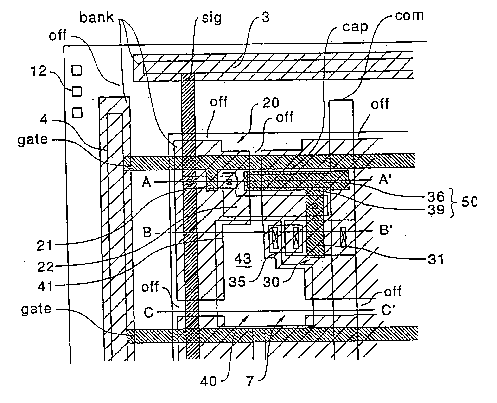
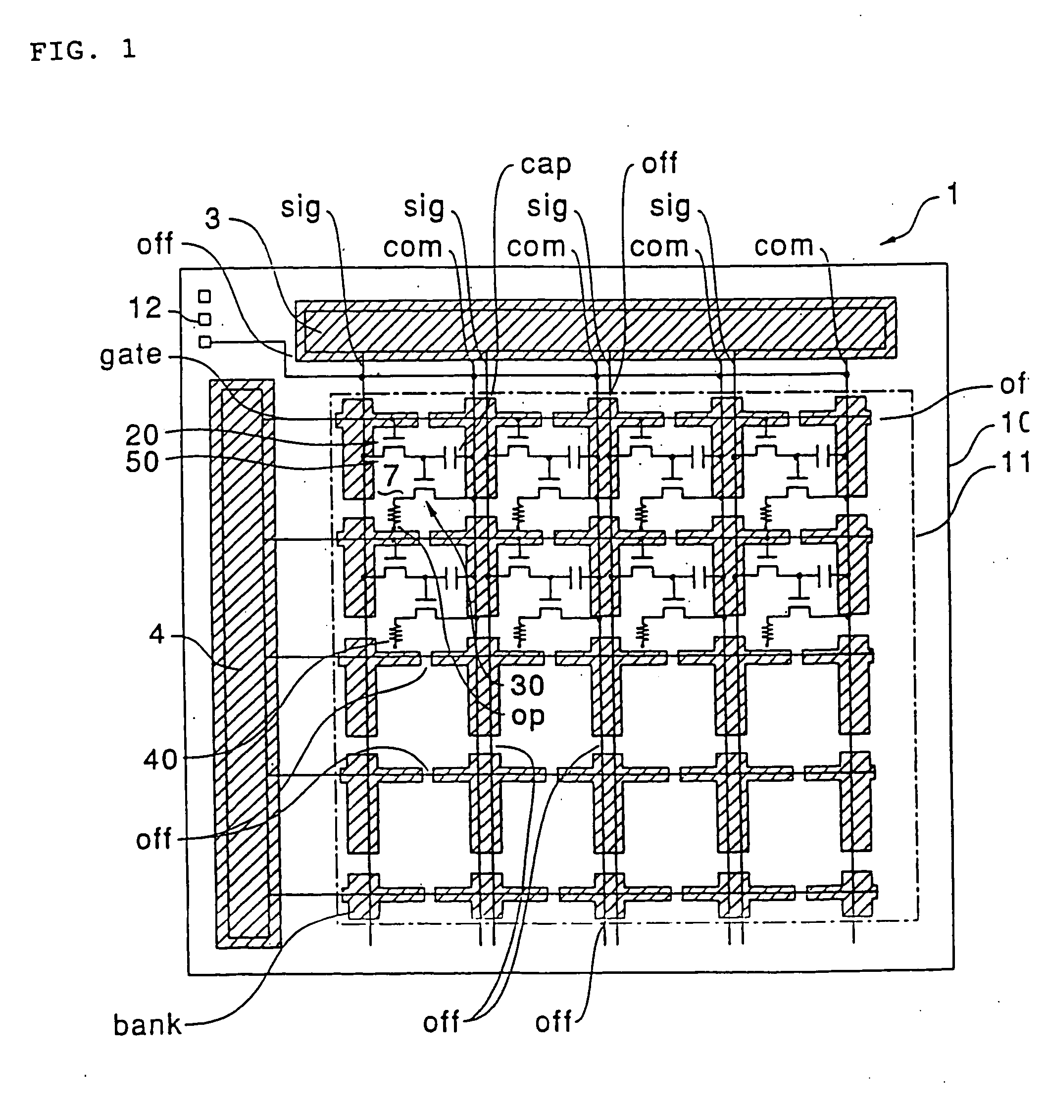
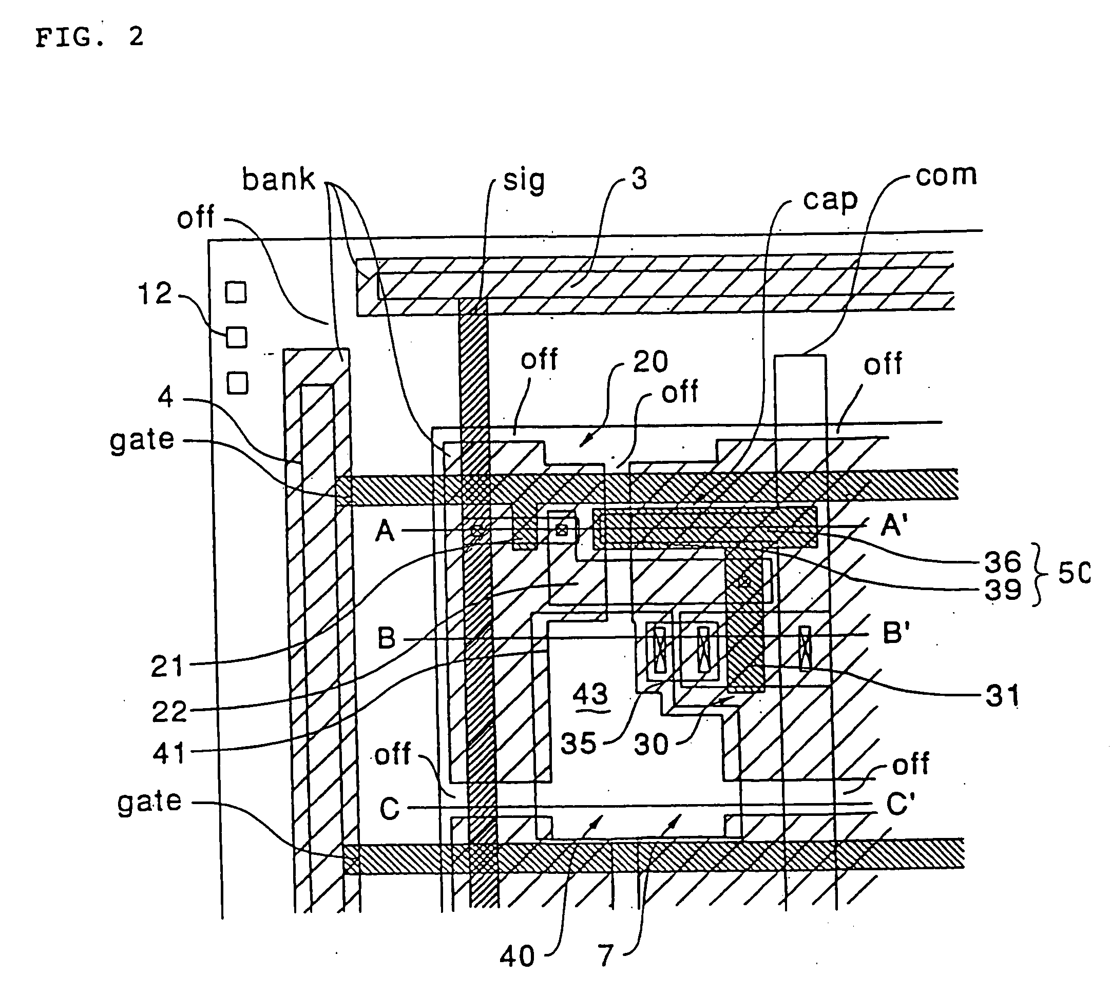
[0074]FIG. 7 is a block diagram which schematically shows the general layout of an active matrix display device. FIG. 8 is a plan view which shows a pixel included in the device shown in FIG. 7. FIGS. 9(A), 9(B), and 9(C) are sectional views taken along the line A-A′, the line B-B′, and the line C-C′ of FIG. 8, respectively. Since this embodiment has basically the same configuration as that of embodiment 1, the same reference numerals are used for the parts that are the same as those of embodiment 1, and detailed description thereof will be omitted.

[0075] As shown in FIG. 7, FIG. 8, and FIGS. 9(A), 9(B), and 9(C), in an active matrix display device 1 of this embodiment, a thick insulating film composed of a resist film (bank layer bank, a shaded region in which lines that slant to the left are drawn at a large pitch) is also provided along the data lines sig and the scanning lines gate, and the opposing electrode op is formed on the upper layer side of th...

embodiment 2

[0080]FIG. 10 is a block diagram which schematically shows the general layout of an active matrix display device. FIG. 11 is a plan view which shows a pixel included in the device shown in FIG. 10. FIGS. 12(A), 12(B), and 12(C) are sectional views taken along the line A-A′, the line B-B′, and the line C-C′ of FIG. 11, respectively. Since this embodiment basically has the same configuration as that of embodiment 1, the same reference numerals are used for the parts that are the same as those of embodiment 1, and detailed description thereof will be omitted.

[0081] As shown in FIG. 10, FIG. 11, and FIGS. 12(A), 12(B), and 12(C), in an active matrix display device 1 of this embodiment, a thick insulating film composed of a resist film (bank layer bank, a shaded region in which lines that slant to the left are drawn at a large pitch) is formed in a strip along the data lines sig, and the opposing electrode op is formed on the upper layer side of the bank layer bank. Thereby, since the s...


PUM


Abstract

In order to provide an active matrix display device in which parasitic capacitance or the like is suppressed by forming a thick insulating film around an organic semiconductor film and disconnection or the like does not occur in the opposing electrode formed on the upper layer of the thick insulating film, in an active matrix display device, first, a bank layer composed of a resist film is formed along data lines and scanning lines, and by depositing an opposing electrode of a thin film luminescent element on the upper layer side of the bank layer, capacitance that parasitizes the data lines can be suppressed. Additionally, a discontinuities portion is formed in the bank layer. Since the discontinuities portion is a planar section which does not have a step due to the bank layer, disconnection of the opposing electrode does not occur at this section. When an organic semiconductor film is formed by an ink jet process, a liquid material discharged from an ink jet head is blocked by the bank layer.

Description

[0001] This is a Divisional Application of application Ser. No. 10 / 442,057 filed May 21, 2003 which is a Continuation of application Ser. No. 09 / 993,565 filed Nov. 27, 2001. The entire disclosures of the prior applications are hereby incorporated by reference herein in their entirety.BACKGROUND OF THE INVENTION [0002] 1. Field of the Invention [0003] The present invention relates to an active matrix display device in which a thin film luminescent element such as an EL (electroluminescence) element or LED (light emitting diode) element, that emits light by application of a driving current to an organic semiconductor film, is driven and controlled by a thin film transistor (hereinafter referred to as a TFT). [0004] 2. Description of the Related Art [0005] Active matrix display devices using current-controlled luminescent elements such as EL elements or LED elements have been disclosed. Since luminescent elements used in display devices of this type are self-luminescent, backlights are...

Claims


Application Information

Patent Timeline
Patent Type & Authority Applications(United States)
IPC IPC(8): G09G3/20G09F9/30G09F9/33H05B33/22H01L27/32H01L51/00H01L51/40H01L51/50H05B33/26
CPCG09G3/3225G09G2300/0426G09G2300/0439G09G2300/0842H01L51/5284H01L27/3246H01L27/3276H01L51/0005G09G2320/0223H10K71/135H10K59/122H10K59/131H10K50/865G09F9/30
Inventor YUDASAKA, ICHIO
Owner INTELLECTUAL KEYSTONE TECH LLC
Why Eureka
Try Eureka