Semiconductor memory

Inactive Publication Date: 2008-02-14
SOCIONEXT INC
View PDF12 Cites 8 Cited by
  • Summary
  • Abstract
  • Description
  • Claims
  • Application Information

AI Technical Summary

Benefits of technology

[0017] An objective of the present invention is to provide a semiconductor memory which has flip-flop type memory cells wherein writing of data in memory cells is easier and the cycle time is reduced.
[0020] With the above features, it is possible to provide an appropriate potential to a high-data retaining supply line pair, so that writing in a memory cell becomes easy. Therefore, high speed writing is stably performed even when the supply voltage is low. A high-data retaining supply circuit receives a signal determined according to an input data signal and address signal without the intervention of a bit line and drives a high-data retaining supply line connected to the high-data retaining supply circuit according to the received signal. Thus, high speed writing is possible.
[0021] According to the present invention, in a semiconductor memory having flip-flop type memory cells (e.g., SRAMs), writing becomes easy, and the cycle time is reduced. Therefore, a semiconductor memory which operates on a low supply voltage but which has a large write margin, which is capable of high speed operation, and which has stable memory cell characteristics, can be realized.

Problems solved by technology

For example, in a semiconductor memory which has flip-flop type memory cells, such as static random access memory (SRAM), it has become very difficult for the memory cells to have stable characteristics due to variations in characteristics of transistors constituting the memory cells or decrease of supply voltage.
Accordingly, the yield of semiconductor memories disadvantageously decreases due to reduction in static noise margin (SNM) or write margin.
However, the semiconductor memory of FIG. 6 disadvantageously requires a long time for writing of data in a memory cell as described below.
Thus, as a result, the time required for writing is long.
In the semiconductor memory of FIG. 6, after writing of data in the memory cell is completed, it disadvantageously takes a long time for the decreased potential of the high-data retaining supply line to return to supply potential VDD as described below.
Thus, the cycle time for writing is also long.

Method used


Image

  • Semiconductor memory
  • Semiconductor memory
  • Semiconductor memory

Examples


embodiment 1

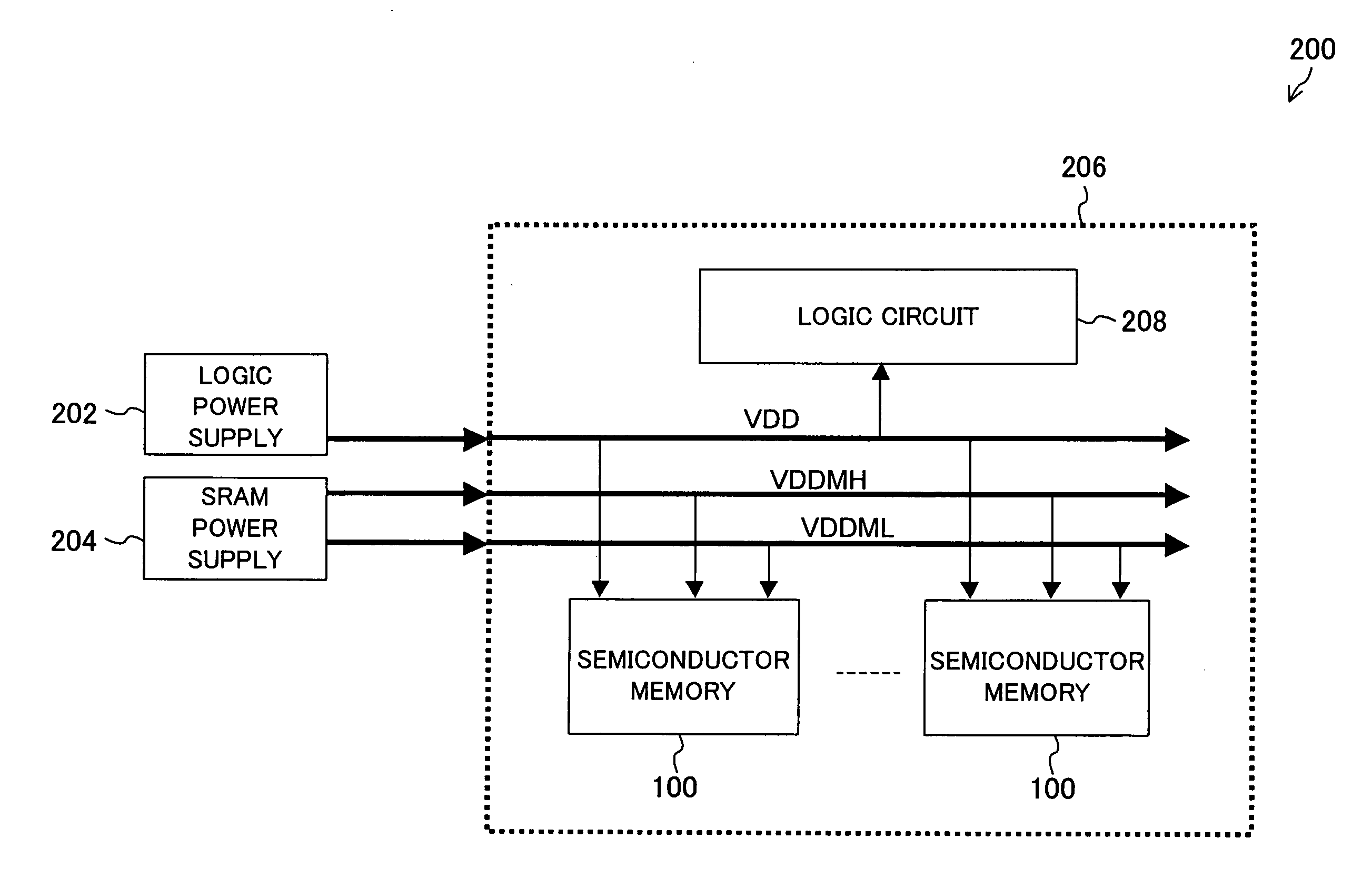
[0030]FIG. 1 is a block diagram showing a structure of a semiconductor circuit system 200 which has a semiconductor memory according to embodiment 1 of the present invention. The semiconductor circuit system 200 includes a power supply for a logic circuit (logic power supply 202), a power supply for SRAM (SRAM power supply 204), and an LSI (large-scale integration) 206. The LSI 206 includes a plurality of semiconductor memories 100 and a logic circuit 208.

[0031] The logic power supply 202 generates supply potential VDD which is supplied to the plurality of semiconductor memories 100 and the logic circuit 208. The SRAM power supply 204 generates high-data retaining supply potentials VDDMH and VDDML for retaining high data in memory cells, which are supplied to the plurality of semiconductor memories 100. High-data retaining supply potential VDDMH is higher than supply potential VDD. High-data retaining supply potential VDDML is lower than supply potential VDD.

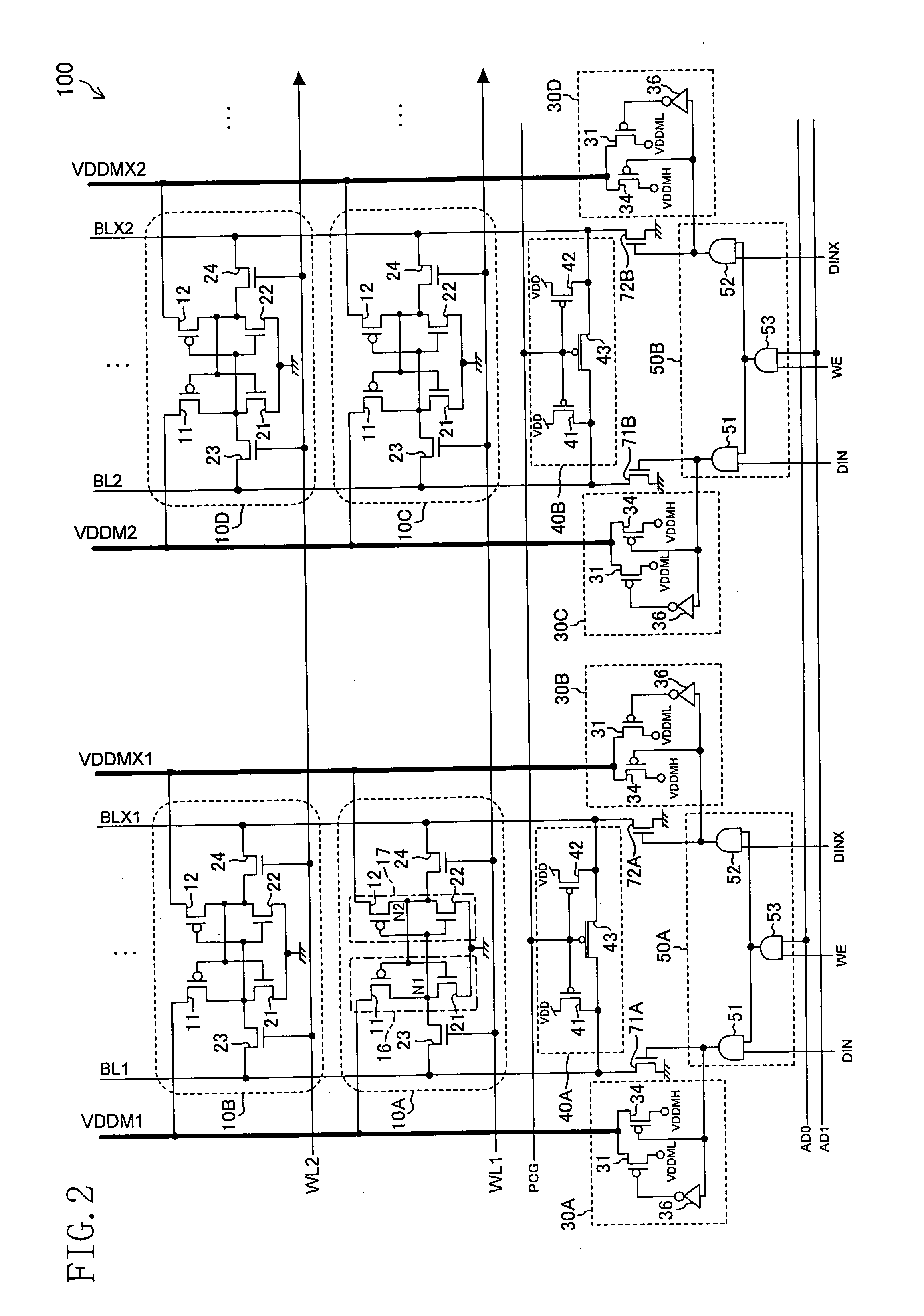
[0032]FIG. 2 is a circ...

embodiment 2

[0074]FIG. 4 is a block diagram showing a structure of a semiconductor circuit system 400 which has a semiconductor memory according to embodiment 2 of the present invention. The semiconductor circuit system 400 includes a power supply for a logic circuit (logic power supply 202), a power supply for SRAM (SRAM power supply 404), and an LSI 406. The LSI 406 includes a plurality of semiconductor memories 300 and a logic circuit 208.

[0075] The logic power supply 202 generates supply potential VDD which is supplied to the plurality of semiconductor memories 300 and the logic circuit 208. The SRAM power supply 404 generates high-data retaining supply potential VDDMH which is supplied to the plurality of semiconductor memories 300. High-data retaining supply potential VDDMH is higher than supply potential VDD.

[0076]FIG. 5 is a circuit diagram showing a structure of a semiconductor memory 300 according to embodiment 2 of the present invention. The semiconductor memory 300 has substantial...


PUM


Abstract

A semiconductor memory includes a plurality of memory cells, each of which includes a first inverter connected to one of high-data retaining supply lines which constitute one of high-data retaining supply line pairs corresponding to the memory cell and a second inverter connected to the other one of the high-data retaining supply lines which constitute the corresponding high-data retaining supply line pair, an input and output of the second inverter being connected to an output and input of the first inverter, respectively. A selected high-data retaining supply circuit receives a signal determined according to an input data signal and address signal without the intervention of any of the bit lines which constitute the bit line pairs to drive the connected high-data retaining supply lines such that it has a potential corresponding to the received signal.

Description

CROSS-REFERENCE TO RELATED APPLICATIONS [0001] This application claims priority under 35 U.S.C. §119(a) on Japanese Patent Application No. 2006-219589 filed on Aug. 11, 2006 and Japanese Patent Application No. 2007-199707 filed on Jul. 31, 2007, the entire contents of which are hereby incorporated by reference. BACKGROUND OF THE INVENTION [0002] The present invention relates to a semiconductor memory which has a flip-flop type memory cell and specifically to control of a supply potential which is to be supplied to a memory cell. [0003] In recent years, progress of semiconductor processes has been enhancing finer circuitry and, hence, rapid advance in achieving reduced circuit area of semiconductor integrated circuits and lower supply voltages. For example, in a semiconductor memory which has flip-flop type memory cells, such as static random access memory (SRAM), it has become very difficult for the memory cells to have stable characteristics due to variations in characteristics of ...

Claims


Application Information

Patent Timeline
IPC IPC(8): G11C7/00
CPCG11C11/413
Inventor SUZUKI, TOSHIKAZUISHIKURA, SATOSHI
Owner SOCIONEXT INC
Why Eureka
Try Eureka