Semiconductor memory and system
a technology of semiconductors and memory, applied in the field of semiconductor memory, can solve problems such as failure of disconnection, reduction of yield, and inability to fully perform test on a real signal line adjacent to the dummy signal lin
- Summary
- Abstract
- Description
- Claims
- Application Information
AI Technical Summary
Benefits of technology
Problems solved by technology
Method used
Image
Examples
first embodiment
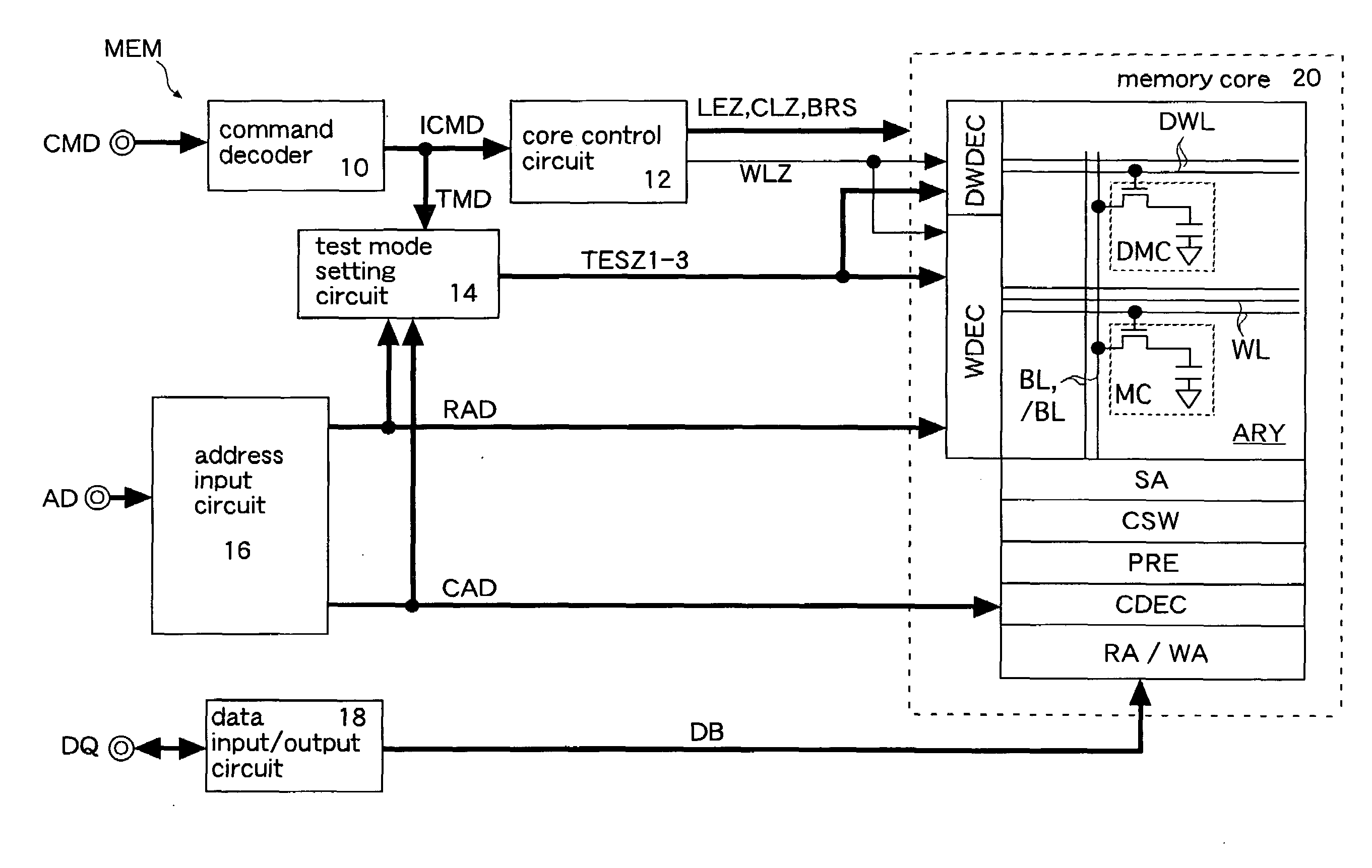
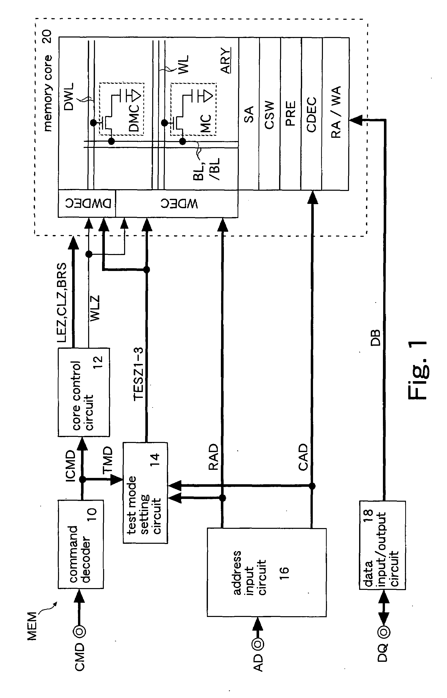
[0042]FIG. 1 shows the present invention. A semiconductor memory MEM is, for example, an FCRAM (Fast Cycle RAM). The FCRAM is a pseudo SRAM including DRAM memory cells and including an SRAM interface. The memory MEM includes a command decoder 10, a core control circuit 12, a test mode setting circuit 14, an address input circuit 16, a data input / output circuit 18, and a memory core 20. Further, to automatically perform a refresh operation of a memory cell MC, the semiconductor memory MEM includes a refresh timer to generate an internal refresh request, a refresh address counter to generate a refresh address, and so on (not shown). Since the present invention does not relate to control of the refresh operation, circuits and operations related to the refresh operation will not be described.
[0043]The command decoder 10 outputs an internal command signal ICMD (read command, write command), a test mode command TMD, and so on in response to a command signal CMD (for example, a chip enable...
second embodiment
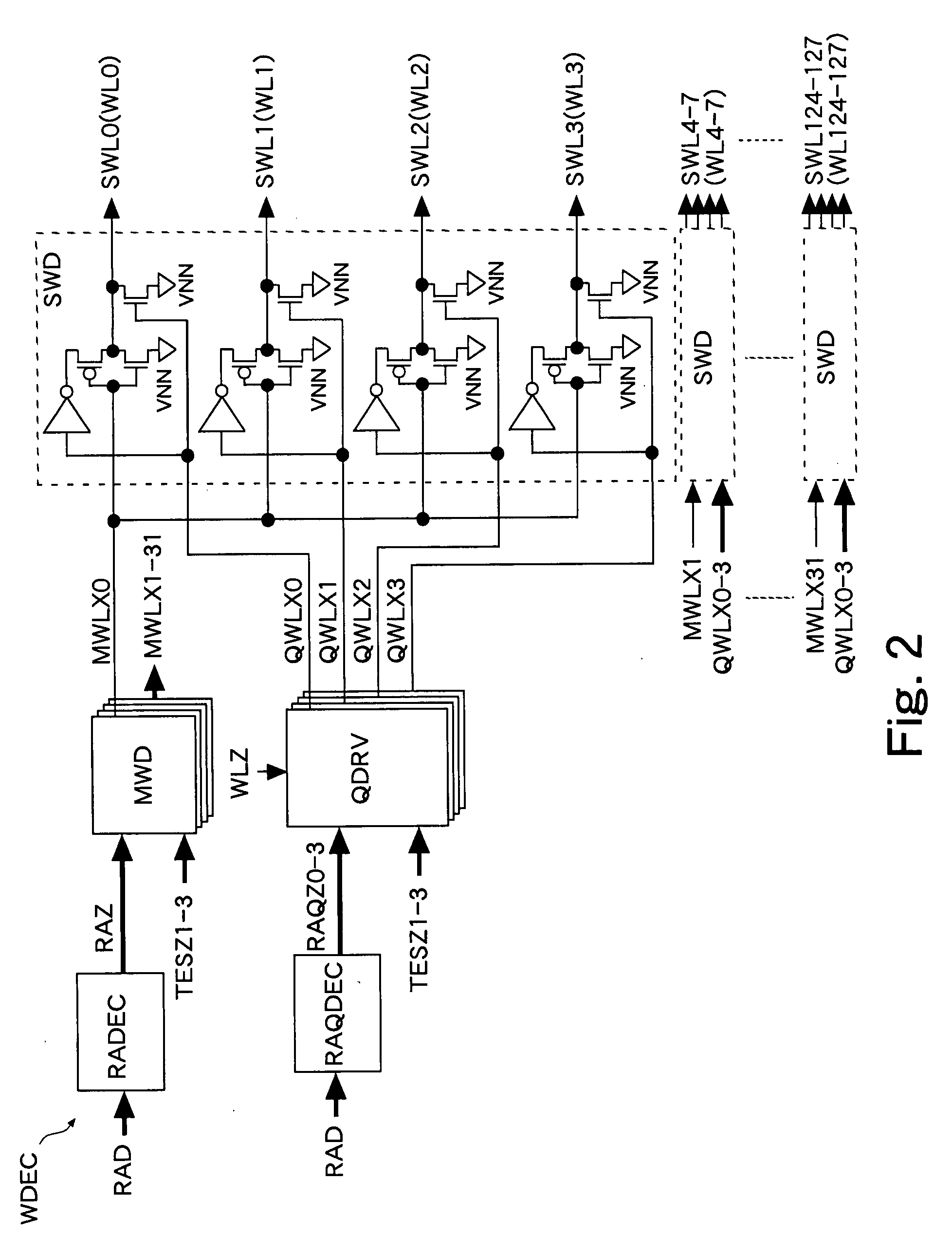
[0056]FIG. 3 shows details of the dummy word decoder DWDEC shown in FIG. 1. A detailed description of circuits having the same configurations as those of the word decoder WDEC shown in FIG. 2 is omitted. The dummy word decoder DWDEC includes dummy main word decoders DMWD and dummy sub-word decoders DSWD. The dummy main word decoder DMWD has the same circuit configuration as the real main word decoder MWD shown in FIG. 2 except that a terminal receiving a dummy decode signal DRAZ is connected to a power supply line V11. The dummy sub-word decoder DSWD has the same circuit configuration as the real sub-word decoder SWD and receives the real sub-word activation signals QWLX0-3. Incidentally, as will be described in a second embodiment and so on discussed later, the dummy decode signal DRAZ is used when data is inputted / outputted to / from the dummy memory cell MC.
[0057]The dummy main word decoders DMWD activate the dummy main word lines DMWLX (DMWLX0-1) to a low logic level in response t...
sixth embodiment
[0116]FIG. 20 shows an operation of the memory MEM in the test mode of the In this embodiment, by the setting of the test mode setting circuit 14E, the operation mode is shifted from the normal operation mode to the test mode, and only the test control signal TESZ5 is activated to a high logic level. The memory MEM performs a fifth stress test, for example, in response to the access command from the memory control unit MCNT shown in FIG. 6 or FIG. 7.
[0117]In response to the access command (write command, for example), the precharge control signal BRS is inactivated to a low logic level, and the word line WL is activated. The number of word lines WL to be activated may be one which corresponds to the row address RAD, or all of the word lines WL may be activated. Incidentally, when no stress is given to the memory cells MC and DMC, the word line WL may not be activated. In this case, by supplying the test mode command TMD to start / end the test to the core control circuit 12E, the sen...
PUM
 Abstract
Description
Claims
Application Information


