Vertical field effect transistor arrays and methods for fabrication thereof

a technology of vertical field effect transistors and transistor arrays, applied in the direction of transistors, semiconductor devices, electrical equipment, etc., can solve the problem that the channel properties of vertical field effect transistor devices are not always optimal for multiple applications, and achieve the effect of improving the efficiency of the transistor array

Inactive Publication Date: 2008-03-06
TAIWAN SEMICON MFG CO LTD
View PDF12 Cites 168 Cited by
  • Summary
  • Abstract
  • Description
  • Claims
  • Application Information

AI Technical Summary

Benefits of technology

[0016]A vertical field effect transistor array semiconductor structure in accordance with the invention includes a plurality of semiconductor pillars. Within the semiconductor structure, all vertical portions of each semiconductor pillar have a semiconductor pillar linewidth greater than a separation distance from an adjacent semiconductor pillar.
[0017]Another vertical field effect transistor array semiconductor structure in accordance with the invention also includes a plurality of semiconductor pillars, where all vertical portions of each semiconductor pillar have a semiconductor pillar linewidth greater than a separation distance from an adjacent semiconductor pillar. Within this other semiconductor structure, at least one semiconductor pillar has a first linewidth and at least one other semiconductor pillar has a second linewidth different than the first linewidth.
[0018]A method for fabricating a vertical field effect transistor array semiconductor structure in accordance with the invention includes forming a plurality of identically sized mask layers located upon a semiconductor substr

Problems solved by technology

Such an offset in scaling is not achievable for a planar field effect transistor since scaling of such a planar device occurs in both a lateral planar direction and a

Method used


Image

  • Vertical field effect transistor arrays and methods for fabrication thereof
  • Vertical field effect transistor arrays and methods for fabrication thereof
  • Vertical field effect transistor arrays and methods for fabrication thereof

Examples


first embodiment

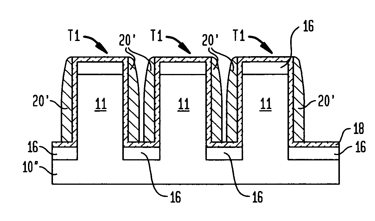
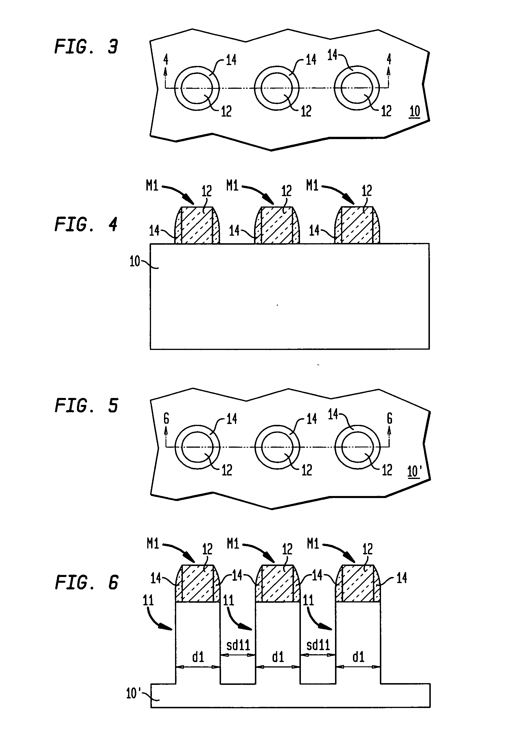
[0024]FIG. 1 to FIG. 10 show a series of schematic cross-sectional and schematic plan-view diagrams illustrating the results of progressive stages in fabricating a semiconductor structure in accordance with an embodiment of the invention. This particular embodiment of the invention comprises the invention. The semiconductor structure whose schematic cross-sectional and schematic plan-view diagrams are illustrated in FIG. 1 to FIG. 10 comprises a vertical field effect transistor device array, and in particular a surrounding gate transistor (SGT) array.

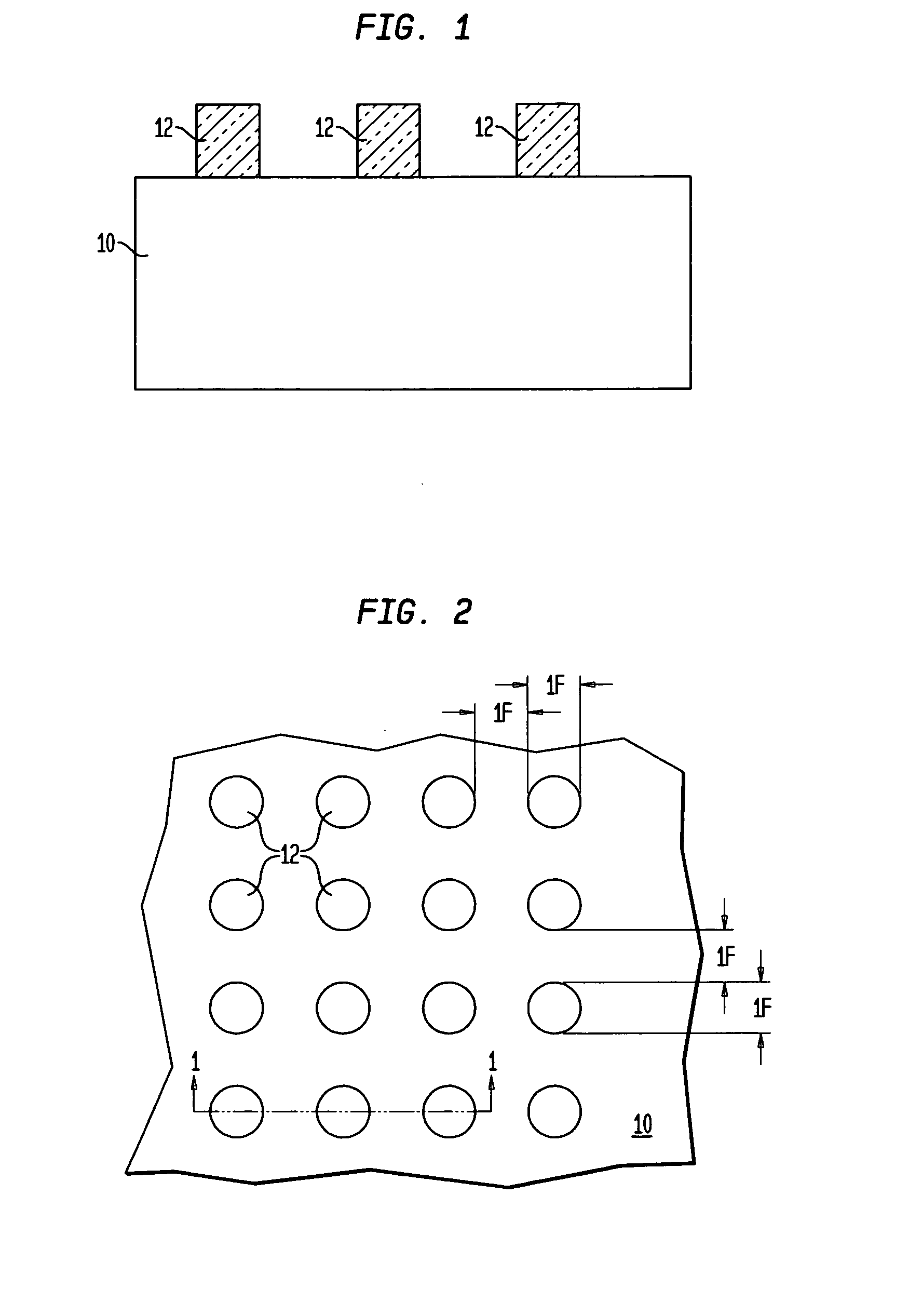
[0025]FIG. 1 shows a schematic cross-sectional diagram of the semiconductor structure at an early stage of the fabrication of the vertical field effect transistor array therein in accordance with the first embodiment.

[0026]FIG. 1 shows a semiconductor substrate 10. A plurality of first pillar mask layers 12 is located upon the semiconductor substrate 10.

[0027]The semiconductor substrate 10 may comprise any of several semiconductor mater...

second embodiment

[0057]FIG. 11 to FIG. 21 show a series of schematic cross-sectional diagrams illustrating the results of progressive stages in fabricating a semiconductor structure in accordance with another embodiment of the invention. This other embodiment of the invention comprises the invention. The semiconductor structure fabricated in accordance with this other embodiment of the invention also comprises a vertical field effect transistor array, and more specifically a surrounding gate transistor (SGT) array.

[0058]FIG. 11 shows a schematic cross-sectional diagram of the semiconductor structure at an early stage in the fabrication thereof in accordance with this other embodiment of the invention.

[0059]FIG. 11 is generally similar to FIG. 4, with like structures and layers being designated identically numerically. However, FIG. 11 also illustrates a plurality of second pillar mask layers 13 located aligned upon the plurality of first pillar mask layers 12. The plurality of second pillar mask lay...


PUM


Abstract

Vertical field effect transistor semiconductor structures and methods for fabrication of the vertical field effect transistor semiconductor structures provide an array of semiconductor pillars. Each vertical portion of each semiconductor pillar in the array of semiconductor pillars has a linewidth greater than a separation distance to an adjacent semiconductor pillar. Alternatively, the array may comprise semiconductor pillars with different linewidths, optionally within the context of the foregoing linewidth and separation distance limitations. A method for fabricating the array of semiconductor pillars uses a minimally photolithographically dimensioned pillar mask layer that is annularly augmented with at least one spacer layer prior to being used as an etch mask.

Description

BACKGROUND[0001]1. Field of the Invention[0002]The invention relates generally to vertical field effect transistors. More particularly, the invention relates to vertical field effect transistor arrays with enhanced performance.[0003]2. Description of the Related Art[0004]Planar field effect transistors are common devices in the semiconductor fabrication art. Planar field effect transistors are readily fabricated as complementary doped pairs using self aligned methods that use a gate electrode as a self aligned mask for forming source / drain regions into a semiconductor substrate. Planar field effect transistors have been successfully scaled for several decades to increasingly smaller lateral and transverse linewidth dimensions (i.e., linewidth dimensions that are within a plane of a planar transistor, rather than vertical to the plane of the planar transistor).[0005]A recent trend in field effect transistor design and fabrication that competes with the continued trend in planar field...

Claims


Application Information

Patent Timeline
IPC IPC(8): H01L29/94
CPCH01L27/088H01L21/823487H01L29/66666H01L29/7827
Inventor BREITWISCH, MATTHEW J.LAM, CHUNG H.SCHROTT, ALEJANDRO G.
Owner TAIWAN SEMICON MFG CO LTD
Why Eureka
Try Eureka