
Semiconductor stack package for optimal packaging of components having interconnections

a technology of interconnection and stack package, which is applied in the direction of semiconductor devices, semiconductor/solid-state device details, electrical apparatus, etc., can solve the problems of defective chips, high manufacturing cost, and high manufacturing cost of multi-chip packages and multi-chip module packages

Inactive Publication Date: 2008-03-06
SK HYNIX INC
View PDF10 Cites 114 Cited by
  • Summary
  • Abstract
  • Description
  • Claims
  • Application Information

AI Technical Summary

Benefits of technology

[0011]An embodiment of the present invention is directed to a stack package which ensures easy packaging despite a problematic design of interconnections and insufficient interconnection spaces.
[0012]Also, another embodiment of the present invention is directed to a stack package which allows detection of a defective chip prior to implementation of the stacking process, thereby preventing a decrease in the manufacturing yield.

Problems solved by technology

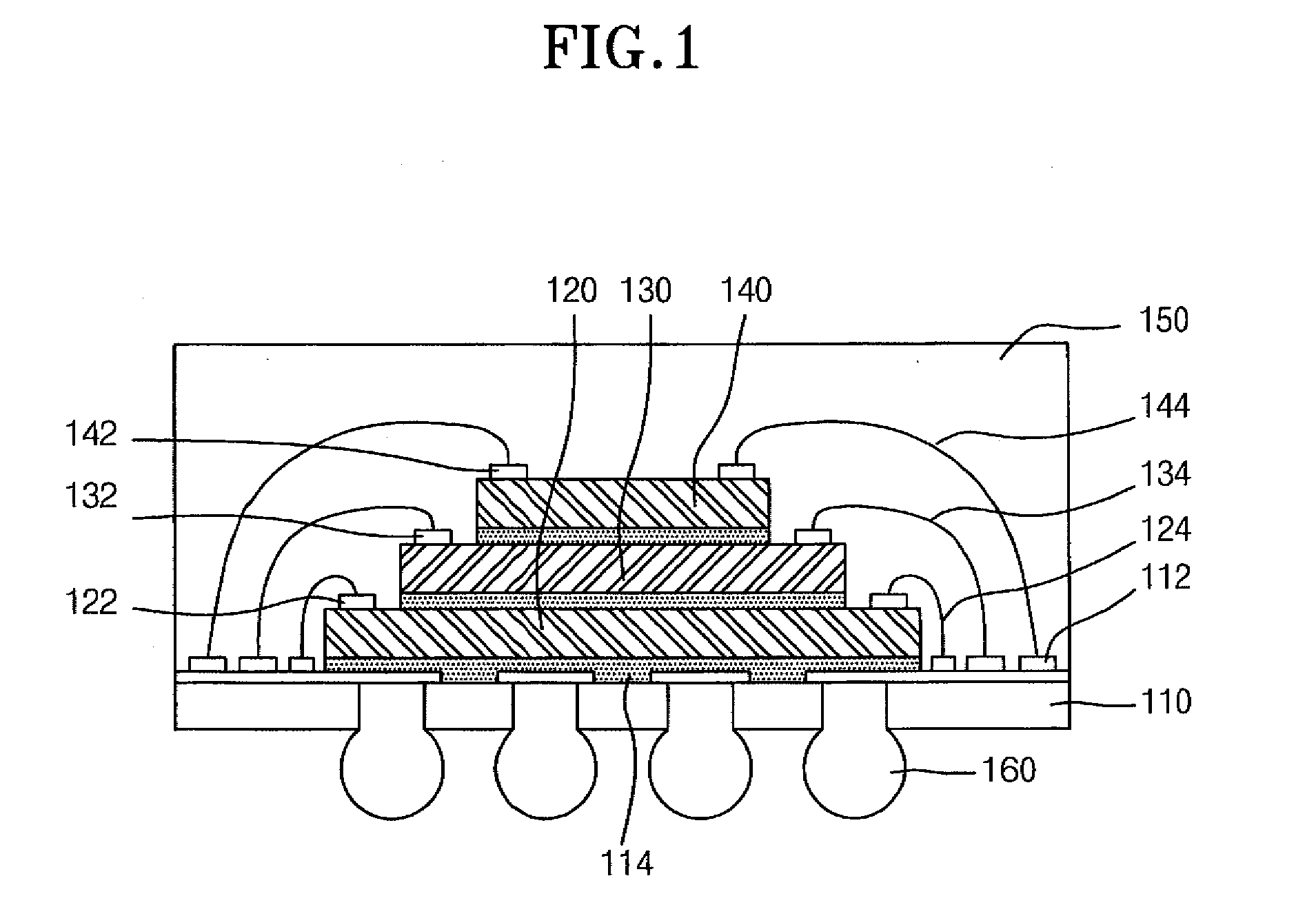
However, the manufacture of a multi-chip package and multi-chip module package is limited because semiconductor chips and packages are mounted so as to be positioned on the same plane of a substrate.
It is difficult to design interconnections for electrically connecting at least two semiconductor chips in the conventional stack chip package, and the bonding wires are likely to be short-circuited due to insufficient interconnection spaces.
A defective chip, generated during the packaging process and burn-in test, cannot be detected until the manufacture process for the stack chip package is completed and the stack package subsequently tested.
Therefore, the manufacturing yield of the product decreases due to the presence of defective chips.

Method used


Image

  • Semiconductor stack package for optimal packaging of components having interconnections
  • Semiconductor stack package for optimal packaging of components having interconnections
  • Semiconductor stack package for optimal packaging of components having interconnections

Examples


first embodiment

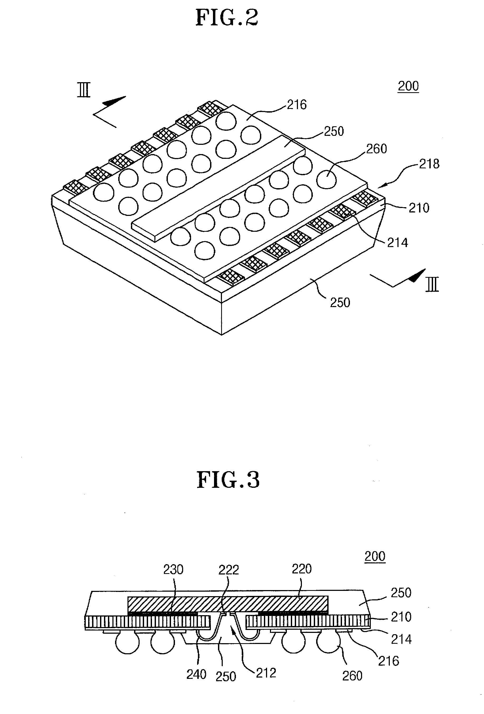
[0033]Hereafter, an FBGA type semiconductor package in accordance with present invention will be described in detail with reference to FIGS. 2 and 3.

[0034]As shown in FIGS. 2 and 3, a substrate 210 has a cavity 212 located at the middle portion thereof. A plurality of conductive patterns 214 is formed on the lower surface of the substrate 210 to extend from positions adjacent to the cavity 212 to the edges of the substrate 210. An insulation layer, preferably, a solder resist 216 is formed on the lower surface of the substrate 210 including the conductive patterns 214. The solder resist 216 has grooves 218 which are defined to expose both end portions and partial areas of the conductive patterns 214. As will be described later in detail, the grooves 218 are defined to form electrical connections between individual semiconductor packages when manufacturing a stack package. Preferably, the grooves 218 are defined in a line type.

[0035]A center pad type semiconductor chip 220, which has...

second embodiment

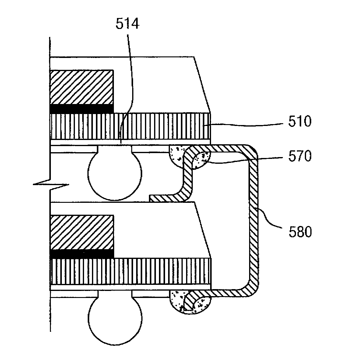
[0048]FIG. 5 is a cross-sectional view illustrating a stack package in accordance with the present invention.

[0049]As shown in the drawing, a stack package 500 has a structure in which first and second FBGA type semiconductor packages 500a and 500b having the same structure as shown in FIG. 3 and determined to lack defective chips through the above-described test are stacked one upon the other.

[0050]Solder pastes 570 serving as conductive adhesives are formed on the exposed end portions of the conductive patterns 514 of the first semiconductor package 500a located upward and on the exposed end portions of the conductive patterns 514 of the second semiconductor package 500b located downward. Clip-shaped conductors 580 are clipped onto the edge portions of the substrate 510 of the downwardly located second semiconductor package 500b. One end of each clip-shaped conductor 580 is connected to the exposed end portions of the conductive patterns 514 of the second semiconductor package 500...

third embodiment

[0056]FIG. 6 is a cross-sectional view illustrating a stack package in accordance with the present invention.

[0057]Referring to FIG. 6, in a stack package 600 in accordance with a third embodiment of the present invention, instead of the solder pastes, solder bumps 670 serving as conductive adhesives are formed on the exposed end portions of conductive patterns 614. By conducting a reflow process, clip-shaped conductors 680 and semiconductor packages 600a and 600b are electrically and mechanically connected to each other by the solder bumps 670.

[0058]Since the remaining component elements of the stack package in accordance with the third embodiment of the present invention, excluding the solder bumps 670, are the same as those of the aforementioned first embodiment, a detailed description thereof will be omitted herein.

[0059]As the conductive adhesives, combinations of solder pastes and solder bumps can be used in place of the solder bumps 670 which are made of single material.


PUM


Abstract

A stack package comprises a first semiconductor package having a substrate which is formed with a plurality of conductive patterns on a lower surface thereof and with an insulation layer on the lower surface thereof including the conductive patterns, the insulation layer having grooves for exposing the portions of the conductive patterns disposed at least both end portions of the substrate; a second semiconductor package located below the first semiconductor package and having the same structure as the first semiconductor package; conductive adhesives formed on the exposed end portions of the conductive patterns of the first and second semiconductor packages; and a plurality of clip-shaped conductors clipped on both ends of the second semiconductor package and having first ends and second ends which electrically and mechanically connect the conductive patterns of the first semiconductor package and the conductive patterns of the second semiconductor package to each other via the conductive adhesives.

Description

CROSS-REFERENCE TO RELATED APPLICATIONS[0001]The present application claims priority to Korean patent application number 10-2006-0083792 filed on Aug. 31, 2006, which is incorporated herein by reference in its entirety.BACKGROUND OF THE INVENTION[0002]The present invention relates to a semiconductor package, and more particularly to a stack package, which ensures easy packaging despite problematic interconnections and insufficient interconnection spaces.[0003]As electronic products become increasingly multi-functional light weight, slim, compact, and miniature, the high-density mounting of packages is required to facilitate such characteristics. In particular, the multi-functional nature of an electronic product necessitates an increased number of packages must be mounted on a substrate of limited size; therefore, various techniques for the high-density mounting of packages have been researched and suggested in the art. Research has also focused on decreasing the size of the package...

Claims


Application Information

Patent Timeline
Patent Type & Authority Applications(United States)
IPC IPC(8): H01L23/02
CPCH01L23/3128H01L2224/06136H01L2224/32145H01L2224/32225H01L2224/4824H01L2224/73215H01L2224/73265H01L2924/15311H01L25/105H01L2225/1052H01L2225/1023H01L2924/00H01L23/12H01L23/48
Inventor KIM, JAE MYUN
Owner SK HYNIX INC
Learn More