Methods of Making Power Semiconductor Devices with Thick Bottom Oxide Layer

a technology of semiconductor devices and oxide layers, applied in the direction of electric variable regulation, process and machine control, instruments, etc., can solve the problems of improving the voltage performance of transistors while maintaining a low rsub>dson /sub>, and achieves improved voltage performance, reduced parasitic capacitance, and high switching speed

Active Publication Date: 2008-06-12
SEMICON COMPONENTS IND LLC
View PDF101 Cites 92 Cited by
  • Summary
  • Abstract
  • Description
  • Claims
  • Application Information

AI Technical Summary

Benefits of technology

[0026]The present invention provides various embodiments for power devices, as well as their methods of manufacture, packaging, and circuitry incorporating the same for a wide variety of power electronic applications. Broadly, one aspect of the invention combines a number of charge balancing techniques and other techniques for reducing parasitic capacitance to arrive at various embodiments for power devices with improved voltage performance, higher switching speed, and lower on-resistance. Another aspect of the invention provides improved termination structures for low, medium and high voltage devices. Improved methods of fabrication for power devices are provided according to other aspects of the invention. Improvements to specific processing steps, such as formation of trenches, formation of dielectric layers inside trenches, formation of mesa structures, processes for reducing substrate thickness, among others are offered by various embodiments of the invention. According to another aspect of the invention, charge balanced power devices incorporate temperature and current sensing elements such as diodes on the same die. Other aspects of the invention improve equivalent series resistance (ESR), or gate resistance, for power devices, incorporate additional circuitry on the same chip as the power device and provide improvements to the packaging of charge balanced power devices.

Problems solved by technology

For example, in the case of the power MOSFET, because of the proportional relationship between the drain-to-source on-resistance RDSon and the breakdown voltage, improving the voltage performance of the transistor while maintaining a low RDSon poses a challenge.

Method used


Image

  • Methods of Making Power Semiconductor Devices with Thick Bottom Oxide Layer
  • Methods of Making Power Semiconductor Devices with Thick Bottom Oxide Layer
  • Methods of Making Power Semiconductor Devices with Thick Bottom Oxide Layer

Examples


Embodiment Construction

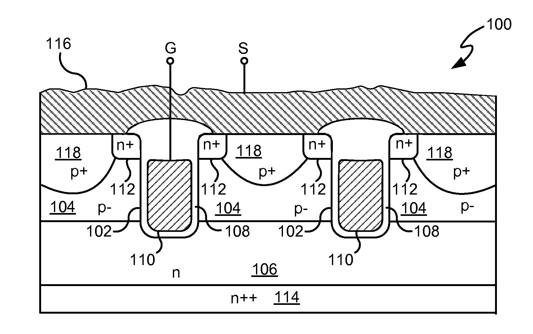
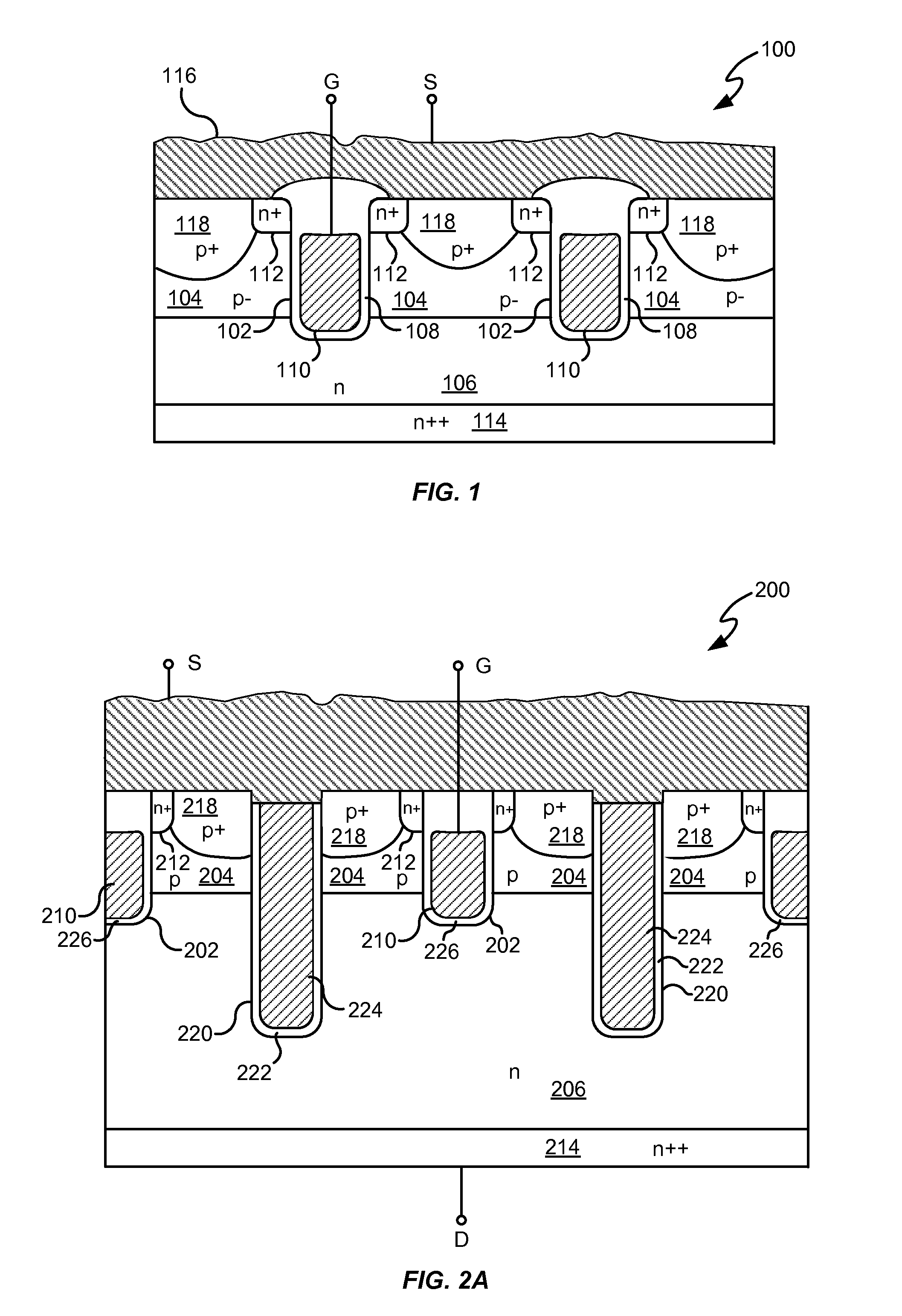
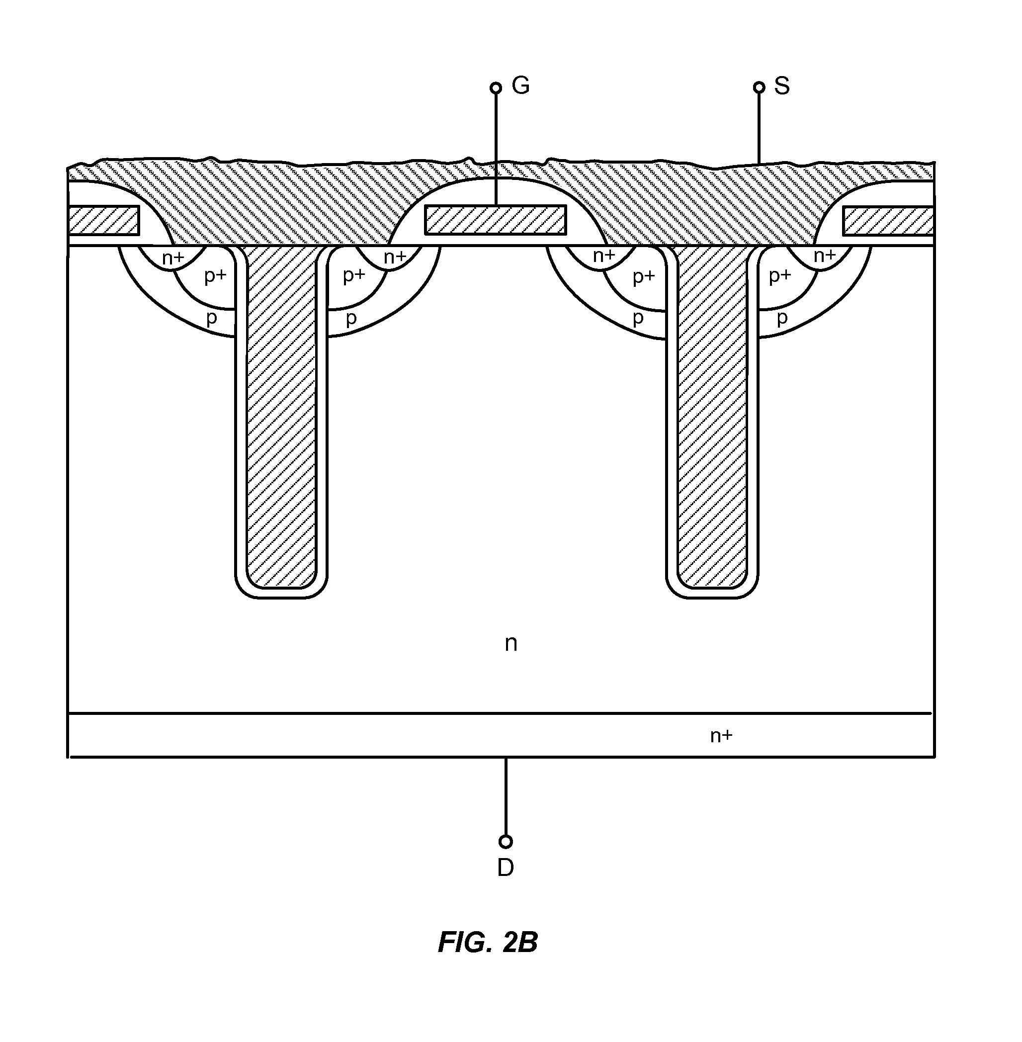
[0109]The power switch can be implemented by any one of power MOSFET, IGBT, various types of thyristors and the like. Many of the novel techniques presented herein are described in the context of the power MOSFET for illustrative purposes. It is to be understood however that the various embodiments of the invention described herein are not limited to the power MOSFET and can apply to many of the other types of power switch technologies, including, for example, IGBTs and other types of bipolar switches and various types of thyristors, as well as diodes. Further, for the purposes of illustration, the various embodiments of the invention are shown to include specific p and n type regions. It is understood by those skilled in the art that the teachings herein are equally applicable to devices in which the conductivities of the various regions are reversed.

[0110]Referring to FIG. 1, there is shown a cross-sectional view of a portion of an exemplary n-type trench power MOSFET 100. As with...


PUM


Abstract

A method for forming thick oxide at the bottom of a trench formed in a semiconductor substrate includes forming a conformal oxide film that fills the trench and covers a top surface of the substrate. and etching the oxide film off the top surface of the substrate and inside the trench to leave a substantially flat layer of oxide having a target thickness at the bottom of the trench. The oxide film can be deposited by sub-atmospheric chemical vapor deposition processes, directional Tetraethoxysilate (TEOS) processes, or high density plasma deposition processes that form a thicker oxide at the bottom of the trench than on the sidewalls of the trench.

Description

CROSS-REFERENCES TO RELATED APPLICATIONS[0001]This application is a continuation of the following commonly-assigned U.S. patent application:[0002]Ser. No. 11 / 026,276, entitled “Power Semiconductor Devices and Methods of Manufacture,” by Challa et al., filed Dec. 29, 2004;[0003]which claims the benefit of the following U.S. Provisional patent application:[0004]No. 60 / 533,790, entitled “Power Semiconductor Devices and Methods of Manufacture,” by Challa et al. filed Dec. 30, 2003;[0005]and is a continuation-in-part of the following commonly-assigned U.S. patent applications:[0006]Ser. No. 10 / 640,742, entitled “Improved MOS Gating Method for Reduced Miller Capacitance and Switching Losses,” by Kocon et al., filed Aug. 14, 2003 (now U.S. Pat. No. 6,870,220);[0007]Ser. No. 10 / 442,670, entitled “Structure and Method for Forming a Trench MOSFET[0008]Having Self-Aligned Features,” by Herrick, filed May 20, 2003 (now U.S. Pat. No. 6,916,745);[0009]and is related to the following commonly-assi...

Claims


Application Information

Patent Timeline
Patent Type & Authority Applications(United States)
IPC IPC(8): H01L21/336H01L21/762G06F1/26H01L21/265H01L21/3065H01L21/311H01L21/68H01L23/495H01L23/498H01L29/06H01L29/165H01L29/40H01L29/417H01L29/423H01L29/49H01L29/78H02M3/00H02M3/335
CPCH01L21/26586H01L21/3065H01L21/30655H01L21/31116H01L21/6835H01L23/4952H01L23/49816H01L29/0623H01L29/0634H01L29/0653H01L29/0661H01L29/0696H01L29/1095H01L29/165H01L29/402H01L29/407H01L29/41766H01L29/4236H01L29/42368H01L29/4238H01L29/4933H01L29/495H01L29/66348H01L29/66734H01L29/7396H01L29/7802H01L29/7804H01L29/7805H01L29/7806H01L29/7811H01L29/7813H01L29/7815H01L29/7828H01L29/7831H01L2221/6834H01L2221/68363H01L2224/16H01L2924/01012H01L2924/01078H01L2924/15311H01L2924/1532H01L2924/19041H01L2924/30105H01L2924/3011H01L2924/3025H02M3/00H02M3/33592H02M7/48Y02B70/1475H01L2924/01019H01L2924/13091H01L2924/13055H01L2924/10253H01L2924/1301H01L2924/13034H01L2924/12032H01L2924/1305H01L2924/00H01L2924/00014Y02B70/10H01L27/0629
Inventor CHALLA, ASHOKELBANHAWY, ALANPROBST, DEAN E.SAPP, STEVEN P.WILSON, PETER H.SANI, BABAK S.LOSEE, BECKYHERRICK, ROBERTMURPHY, JAMES J.MADSON, GORDON K.MARCHANT, BRUCE D.KOCON, CHRISTOPHER B.WOOLSEY, DEBRA S.
Owner SEMICON COMPONENTS IND LLC
Why Eureka
Try Eureka