IC package

a technology of encapsulant and package, applied in the field of ic packages, can solve the problems of serious warpage, inability to avoid curing shrinkage of encapsulant warpage, and still exist warpage, and achieve the effect of enhancing the warpage resistance of the substrate 410 and increasing the young's modulus

Inactive Publication Date: 2008-03-06
POWERTECH TECHNOLOGY
View PDF7 Cites 12 Cited by
  • Summary
  • Abstract
  • Description
  • Claims
  • Application Information

AI Technical Summary

Benefits of technology

[0006]The main purpose of the present invention is to provide an IC package with a stiffening encapsulant which has a larger Young's modulus than the protective encapsulant, moreover, the curing shrinkage of the stiffening encapsulant is smaller than the one of the protecting encapuslant so that the warpage resistance of an IC package can be greatly enhanced. Furthermore, since the stiffening encapsulant is formed in a strip and connects with the chip and protrudes from the bottom surface of the substrate to achieve the warpage resistance of an IC package during encapsulation under a limited package thickness.
[0007]The second purpose of the present invention is to provide an IC package with the cross section of a stiffening encapsulant to enhance package strength.
[0008]The third purpose of the present invention is to provide an IC package with the length of the slot of the substrate to separate the stiffening encapsulant and the protective encapsulant so that both encapsulants with different materials can be molded and cured at the same time without mixing with each other.
[0009]The fourth purpose of the present invention is to provide an IC package with a chip dimension and a die attach material (DAM) to separate the stiffening encapsulant and the protective encapsulant so that both encapsulants with different materials can be molded and cured at the same time without mixing with each other.
[0010]The fifth purpose of the present invention is to provide an IC package with the design of the molding gate to enhance the formation of the stiffening encapsulant.
[0011]The sixth purpose of the present invention is to provide an IC package to prevent the breakage of the bonding wires during thermal cycle tests.

Problems solved by technology

In all kinds of conventional IC packages, warpage is a serious problem existing at various interfaces during packaging processing or in packages.
Therefore, the warpage due to the curing shrinkage of the encapsulant can not be avoided.
The warpage still exists due to the curing shrinkage for both internal encapsulant and external encapsulant during molding process.

Method used


Image

  • IC package
  • IC package
  • IC package

Examples


first embodiment

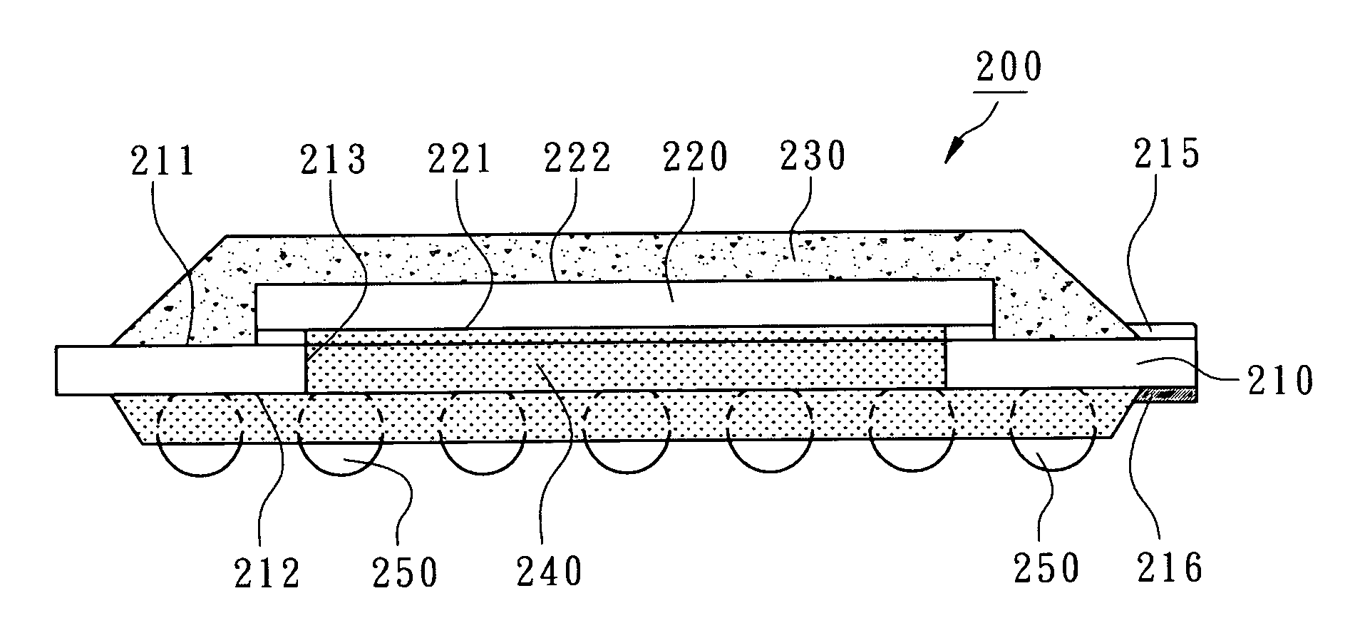
[0028]FIG. 4 to FIG. 8 are shown to illustrate the first embodiment according to the present invention. As shown in FIG. 4 and FIG. 8, an IC package 200, which may be a window BGA, includes a substrate 210, a chip 220, a protective encapsulant 230, at least a stiffening encapsulant 240, and a plurality of external terminals 250. The substrate 210 is an IC carrier with patterned electrical circuits. Normally, the substrate 210 is a printed circuit board or a flexible electrical thin film. The substrate 210 has a top surface 211, a bottom surface 212, and at least a slot 213 where the top surface 211 is designed for die attachment and the bottom surface 212 is designed for external electrical mounting. The slot 213 is in a strip penetrating through the top surface 211 and the bottom surface 212. In the present embodiment, as shown in FIG. 5 and FIG. 6, the substrate 210 is approximately rectangular and has a defined long central axis 214. The slot 213 is aligned with the central line ...

third embodiment

[0038]According to the present invention, an anti-warpage chip carrier for an IC package is revealed, as shown in FIGS. 11 and 12. Before assembly, an anti-warpage chip carrier includes a substrate 410 and at least a rigid stiffener 430 where the substrate 410 has a top surface 411, a bottom surface 412, and at least a slot 413, 414. In the present embodiment, the slot 413 is formed at the center of the substrate 410 and two slots 414 are formed at the edges of the substrate 410. A plurality of bumping pads 415 are formed on the top surface 411 of the substrate 410 and a plurality of ball pads 416 are formed on the bottom surface 412 of the substrate 410 where the bumping pads 415 are electrically connected to the ball pads 416 by internal circuits. In the present embodiment, the substrate 410 is flexible.

[0039]The rigid stiffeners 430 are in a strip and is embedded in the slots 413, 414. The Young's modulus of the rigid stiffener 430 is between 20 GPa and 50 GPa. The material of th...


PUM


Abstract

An IC package mainly includes a substrate having slot(s), a chip, a protective encapsulant, a stiffening encapsulant, and a plurality of external terminals. The Young's modulus of the stiffening encapsulant is greater than the one of the protective encapsulant and the curing shrinkage of the stiffening encapsulant is smaller than the one of the protective encapsulant. The protective encapsulant is formed on one of the surfaces of the substrate for encapsulating the chip. The stiffening encapsulant protrudes from the other surface of the substrate where the external terminals are disposed. Moreover, the stiffening encapsulant is formed inside the slot and is contacted with the chip. Since the stiffening encapsulant is embedded and formed inside the slot, therefore, the contact area of the stiffening encapsulant with the substrate is increased to enhance the warpage resistance of the IC package.

Description

FIELD OF THE INVENTION[0001]The present invention relates to an IC package, and more particularly to a window BGA (Ball Grid Array) package with the enhancement of warpage resistance.BACKGROUND OF THE INVENTION[0002]In all kinds of conventional IC packages, warpage is a serious problem existing at various interfaces during packaging processing or in packages.[0003]As shown in FIG. 1, a window BGA 100 utilizes a substrate 110 having a slot 111 to carry a chip 120 by a die-attaching material 122. The bonding pads 121 of the chip 120 are electrically connected to the substrate 110 by a plurality of bonding wires 150. Then the chip 120 is encapsulated by an encapsulant 130. Moreover, a plurality of external terminals 140 such as solder balls are disposed under the substrate 110 for outer electrical connection. Since the slot 111 of the substrate 110 is formed and aligned to the center line 113 of the substrate 110 and is longer than the chip 120 for filling the slot 111 with the encapsu...

Claims


Application Information

Patent Timeline
Patent Type & Authority Applications(United States)
IPC IPC(8): H01L23/28
CPCH01L23/13H01L23/16H01L23/3128H01L23/3135H01L24/06H01L24/48H01L2224/0401H01L2224/04042H01L2224/05554H01L2224/06136H01L2224/16H01L2224/16225H01L2224/16235H01L2224/32225H01L2224/4824H01L2224/73204H01L2224/73215H01L2924/00014H01L2924/01005H01L2924/01033H01L2924/014H01L2924/14H01L2924/15151H01L2924/15174H01L2924/15311H01L2924/181H01L2924/3511H01L2924/00012H01L2924/00H01L2224/45099H01L2224/45015H01L2924/207
Inventor CHEN, CHENG-PINGFAN, WEN-JENG
Owner POWERTECH TECHNOLOGY
Why Eureka
Try Eureka