Packaged Stacked Semiconductor Device And Method For Manufacturing The Same

a semiconductor device and packaging technology, applied in semiconductor devices, semiconductor/solid-state device details, electrical equipment, etc., can solve the problems of difficult to apply to a semiconductor device mounting process, difficult to form through-electrodes, and conventional techniques that do not disclose wiring on the back surface of three-dimensional stacked semiconductor devices, etc., to achieve the effect of reducing the height of the semiconductor device, reducing the degree of freedom in terms of combination, and low cos

Active Publication Date: 2008-03-13
INVENSAS CORP
View PDF5 Cites 24 Cited by
  • Summary
  • Abstract
  • Description
  • Claims
  • Application Information

AI Technical Summary

Benefits of technology

[0016] According to the present invention, on the back side of the semiconductor device, the tip end surfaces of the through-electrodes can be made flush with the surface of the insulating film, or the tip end surfaces of the through-electrodes can be easily exposed, and subsequently, wiring can be formed through ink jetting by use of metal nanoparticles. Therefore, additional wiring can be formed on the back side at low cost.
[0017] According to the present invention, back wiring on the semiconductor device enables the device to be freely connected (stacked) on another component in three dimensions, and thus the device exhibits drastically increased degree of freedom in terms of combination. Similar to the case of PoP (package on package), which is a currently prevailing technique, the area occupied by the semiconductor device can be reduced by about ⅕ to about 1 / 10, and the height of the semiconductor device can be reduced by about ⅕.
[0018] According to the present invention, the semiconductor devices can be, in principle, infinitely connected in three dimensions, and the device is advantageous in that it can be effectively integrated into three-dimensional sections of small plane area (e.g., the device can be distributed to and integrated at different sections of a robot).
[0019] Although having a size comparable to that of a bare chip, the stacked semiconductor device of the present invention can be subjected to testing satisfactorily. In other words, the semiconductor device can be easily subjected to KGD (known good die) testing. Since the stacked semiconductor device of the present invention is in the form of single complete package, and includes bumps, etc., the device can be brought into reliable contact with a testing jig. That is, the semiconductor device, which has a size equal to that of a conventional bare chip, can be easily subjected to KGD testing for such a bare chip. Therefore, the semiconductor device does not require any additional process or jig, and thus does not cause an increase in cost.
[0020] In the present invention, a nitride film is employed as an insulating film, and the film is formed by use of decomposed species generated through catalytic decomposition of a raw material on a heated catalyst. Therefore, the temperature of an insulating film formation process can be lowered (to 200° C. or lower).
[0021] Thus, in a semiconductor wafer level implementation or semiconductor bare chip stacked structure, an insulating film provided around through-holes of a silicon substrate can be formed through deposition at low temperature. This facilitates formation of through-electrodes required for a considerable decrease in package size.

Problems solved by technology

However, conventional techniques do not disclose wiring on the back surface of a three-dimensional stacked semiconductor device (hereinafter such wiring may be referred to as “back wiring”).
However, such a process requires high-temperature treatment, and thus is difficult to apply to a semiconductor device mounting process.
However, each of the patent documents discloses only a structure whose rigidity is secured by merely a silicon substrate.
Therefore, the structure requires a silicon substrate having a predetermined thickness (e.g., 50 μm or more), and thus requires deep through-holes, leading to difficulty in forming through-electrodes.

Method used


Image

  • Packaged Stacked Semiconductor Device And Method For Manufacturing The Same
  • Packaged Stacked Semiconductor Device And Method For Manufacturing The Same
  • Packaged Stacked Semiconductor Device And Method For Manufacturing The Same

Examples


Embodiment Construction

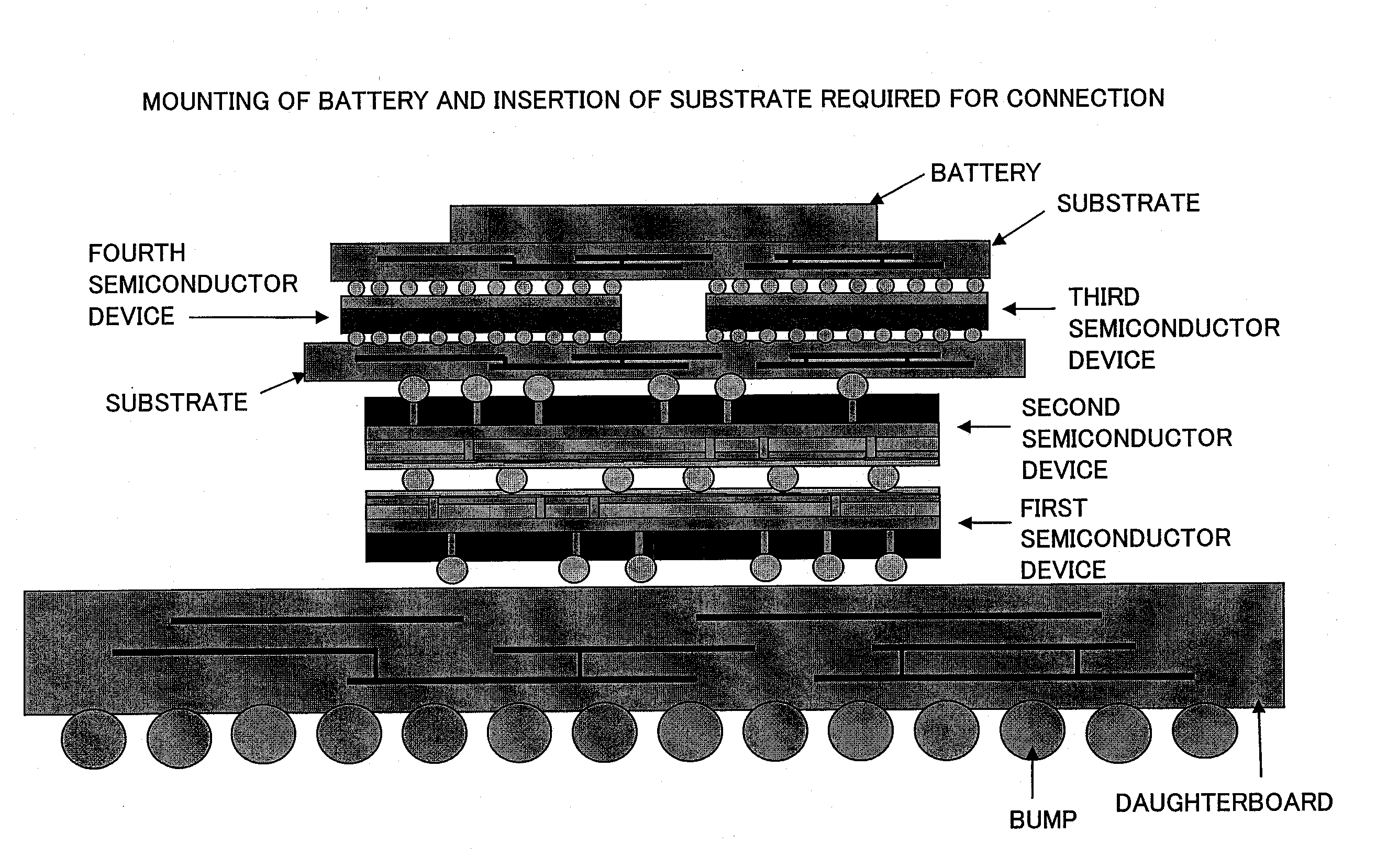
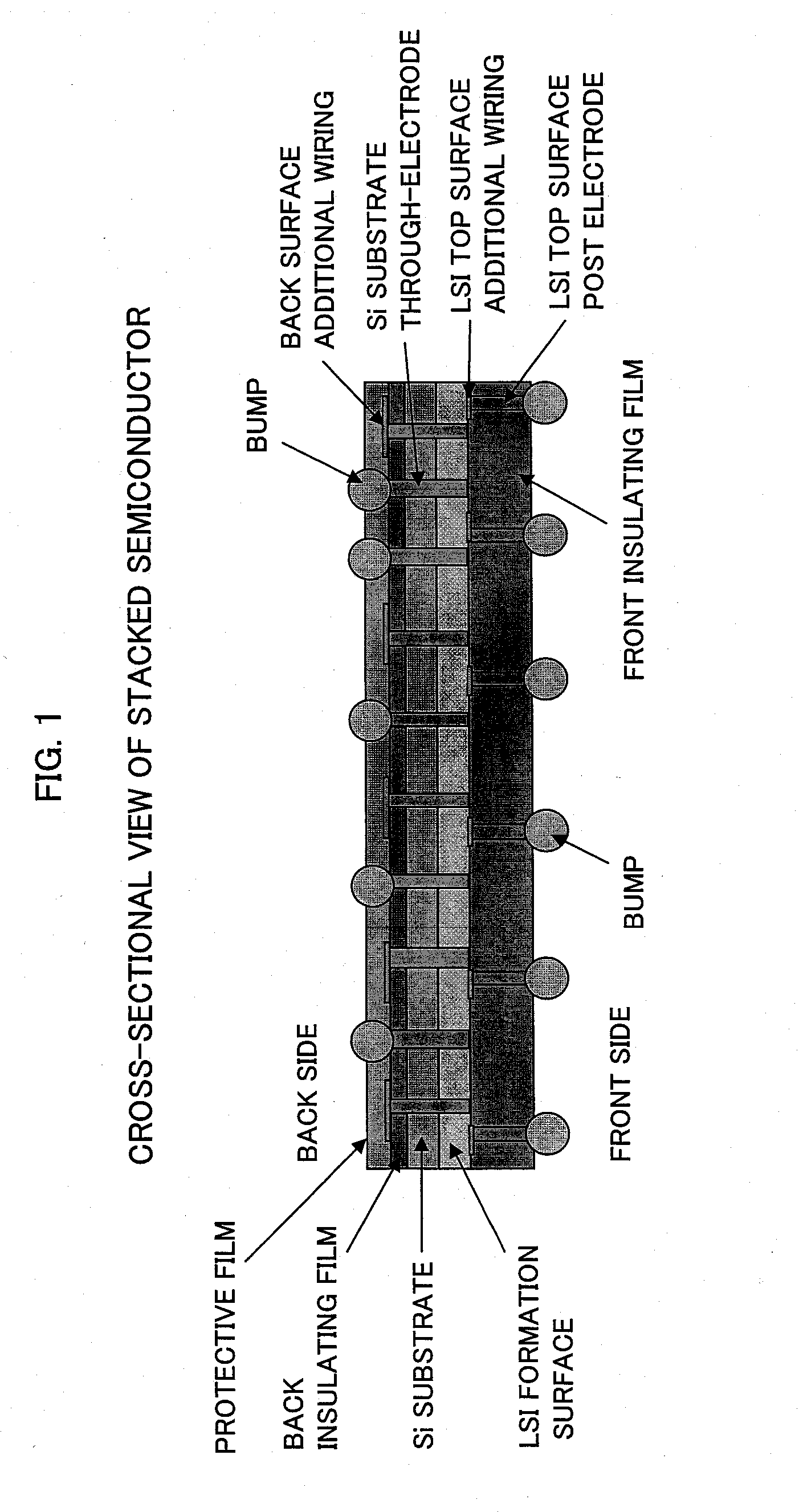
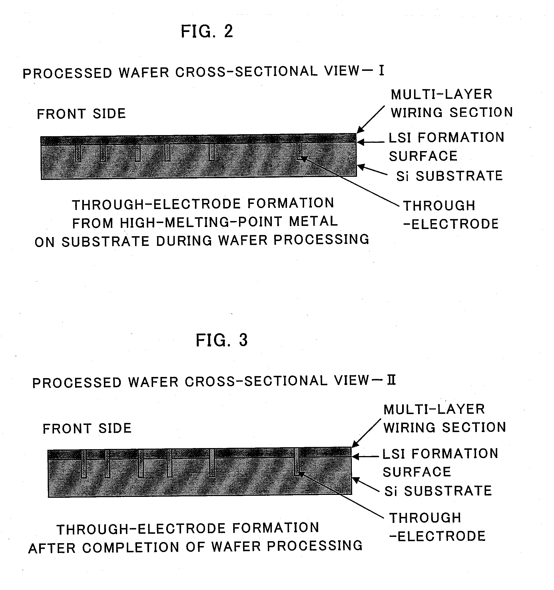
[0053] Before description of the present invention, a three-dimensional stacked semiconductor device which has been previously applied by the present inventors (Japanese Patent Application No. 2003-370651) will be described with reference to FIGS. 29 to 31. FIG. 29 is a cross-sectional view showing the three-dimensional stacked semiconductor device; FIG. 30 is a schematic perspective view showing the entirety of the device; and FIG. 31 shows the bottom surface of the device. As shown in FIG. 29, the three-dimensional stacked semiconductor device includes a first semiconductor device 2 which serves as a bottom unit; a third semiconductor device 4 which serves as a middle unit and is provided and fixated onto the top surface of the first semiconductor device 2; and a second semiconductor device 3 which serves as a top unit and is provided and fixated onto the top surface of the third semiconductor device 4.

[0054] In description of the first, second, and third semiconductor devices 2,...


PUM


Abstract

The present invention provides a packaged stacked semiconductor device which includes bumps serving as external electrode terminals, the bumps being provided on both a front surface and a back surface of the device, and which is sacked on another semiconductor device, substrate, or board having electrode terminals so that the bumps are directly and electrically connected to the electrode terminals. The semiconductor device includes a semiconductor substrate having through-electrodes formed therein. The semiconductor device has, on the front surface side of the semiconductor substrate, a wiring layer connected to the through-electrodes, an insulating film formed on the wiring layer, additional wiring formed on the insulating film, post electrodes connected to the wiring, and external connection bumps connected to the post electrodes. The semiconductor device has, on the back surface side of the semiconductor substrate, an insulating film formed so as to cover the back surface of the semiconductor substrate, exclusive of tip end portions of the through-electrodes, wiring which is formed on the insulating film and to which the through-electrodes are connected, and external connection bumps connected to the wiring.

Description

TECHNICAL FIELD [0001] The present invention relates to a semiconductor device which can be thinned and can be operated at higher speed, and to a method for producing the device. More particularly, the present invention relates to a packaged stacked semiconductor device including a plurality of successively stacked semiconductor devices, and to a method for producing the packaged stacked semiconductor device. BACKGROUND ART [0002] As highly integrated LSI chips have been developed, strong demand has arisen for a decrease in package size, and thus a variety of packaging structures have been proposed. In recent years, attempts have been made to develop a process for forming through-electrodes in semiconductor bare chips, and stacking the semiconductor bare chips. Meanwhile, there is a high likelihood of commercialization of a real-size packaged device having electrodes on its both surfaces. As a variety of multifunctional, small electronic apparatuses have been developed, a semiconduc...

Claims


Application Information

Patent Timeline
Patent Type & Authority Applications(United States)
IPC IPC(8): H01L23/48H01L21/44
CPCH01L21/76898H01L23/3114H01L2924/00014H01L2924/01047H01L2224/45147H01L2924/01019H01L2924/19041H01L23/481H01L25/0657H01L25/50H01L2224/16145H01L2225/06513H01L2225/06517H01L2225/06527H01L2225/06541H01L2225/06572H01L2225/06575H01L2924/01004H01L2924/01046H01L2924/01077H01L2924/01078H01L2924/01079H01L2924/15311H01L2924/00H01L2224/48H01L2224/14181H01L2224/16225H01L2224/17181H01L2224/13025H01L2924/00011H01L2224/05599H01L2924/01005
Inventor ISHIHARA, MASAMICHIIZUMI, AKIRA
Owner INVENSAS CORP
Why Eureka
Try Eureka