Stress sensor for in-situ measurement of package-induced stress in semiconductor devices

a stress sensor and semiconductor technology, applied in the direction of force/torque/work measurement apparatus, semiconductor/solid-state device testing/measurement, instruments, etc., can solve the problems of insufficient accuracy or robustness of strain gauge rosettes, and inability to accurately use non-destructive methods

Inactive Publication Date: 2008-03-20
INTEL CORP
View PDF13 Cites 37 Cited by
  • Summary
  • Abstract
  • Description
  • Claims
  • Application Information

AI Technical Summary

Problems solved by technology

Strain gauge rosettes have been considered for placement on the die, but are not sufficiently accurate or robust at these sma

Method used


Image

  • Stress sensor for in-situ measurement of package-induced stress in semiconductor devices
  • Stress sensor for in-situ measurement of package-induced stress in semiconductor devices
  • Stress sensor for in-situ measurement of package-induced stress in semiconductor devices

Examples


Embodiment Construction

[0027]A stress sensor, methods of making the stress sensor and methods of using the stress sensor are disclosed herein. The stress sensor uses, in one embodiment, carbon nanotubes that are embedded in a surface of a substrate of the die. When stress is induced in the die, the nanotubes respond to the stress. The response of the nanotubes can be measured and correlated to a stress value.

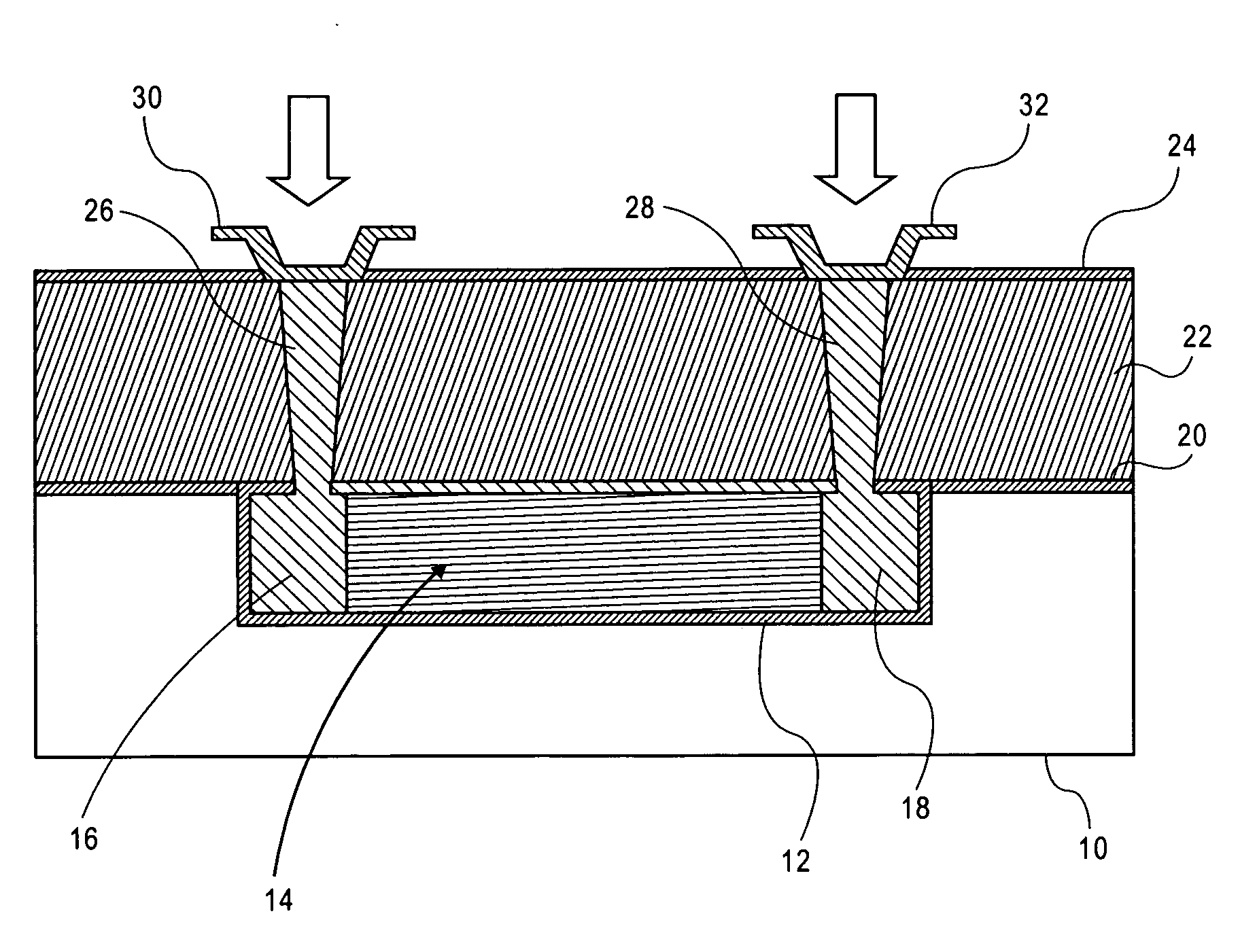
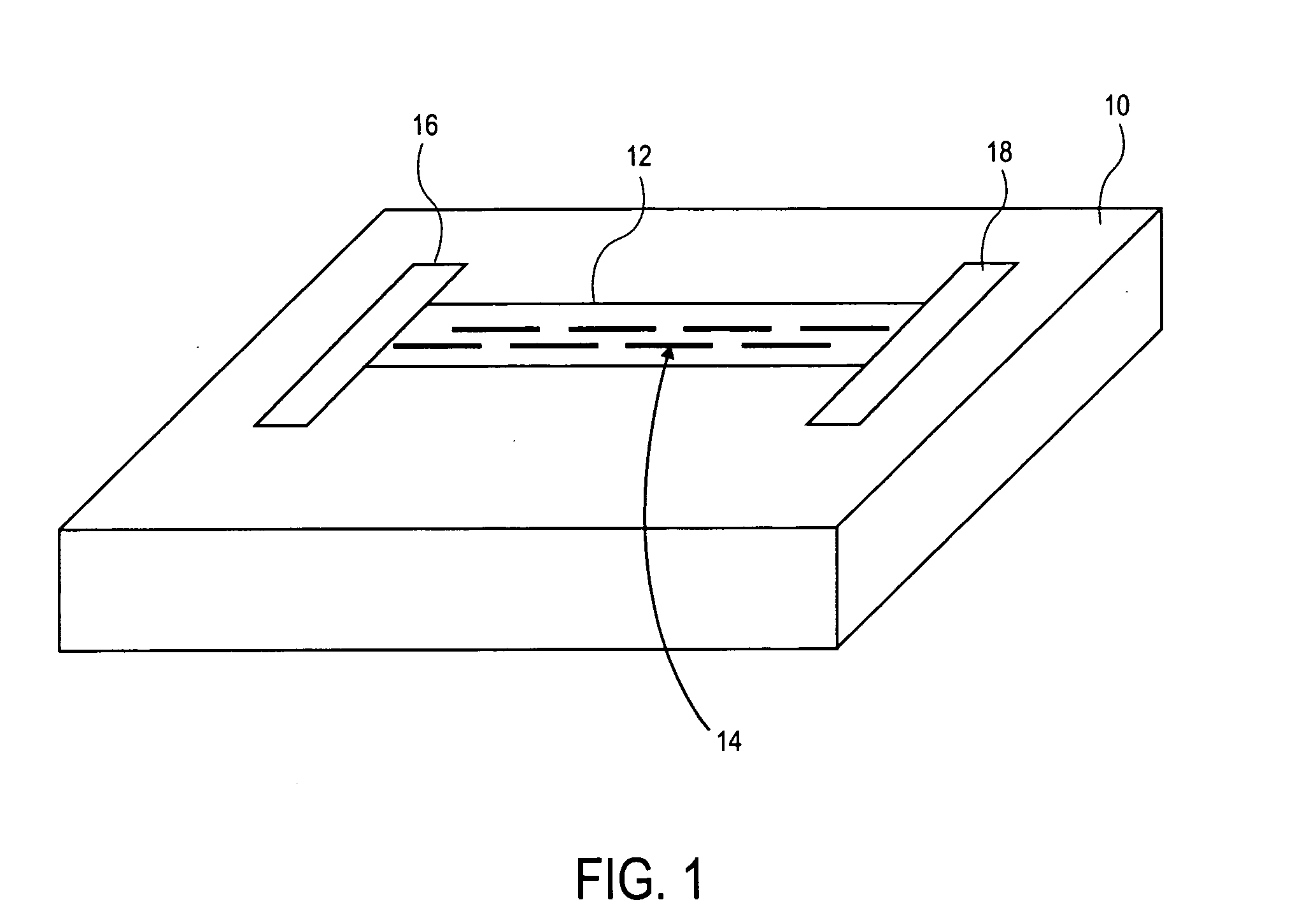
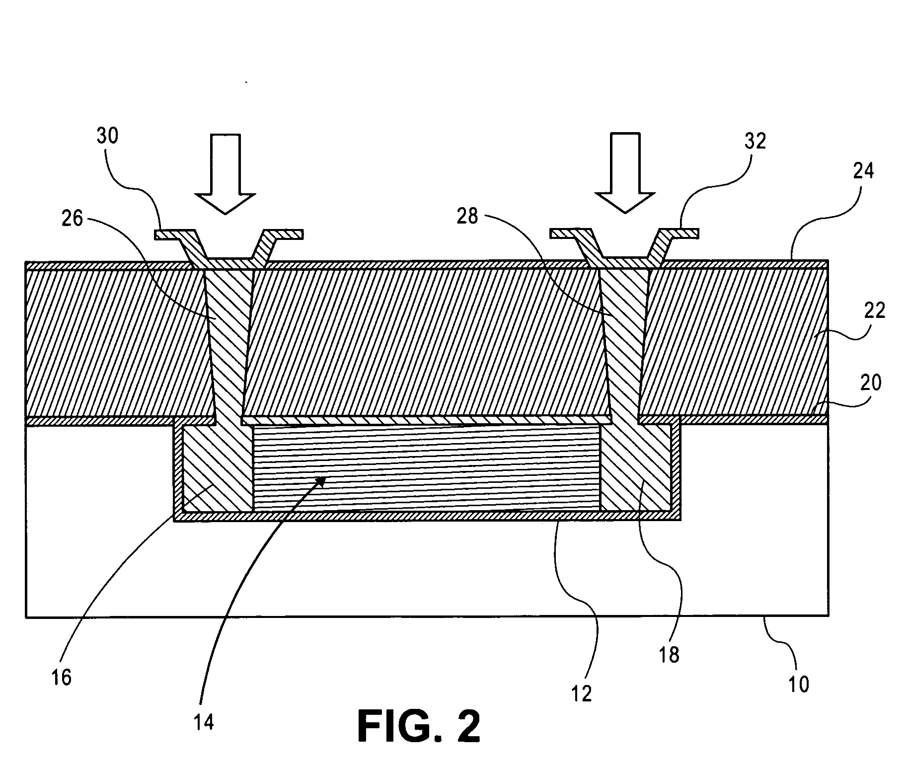
[0028]As shown in FIG. 1 of the accompanying drawings, a stress sensor is included in a die. The die may include any well-known substrate or material on which integrated circuits are typically formed.

[0029]The stress sensor includes a substrate 10, a trench 12, nanotubes 14 and first and second contacts 16, 18. The trench 12 is formed between the first and second contacts 16, 18 and in the substrate 10. The nanotubes 14 are deposited in the trench 12 between the first and second contacts 16, 18. In one embodiment, the nanotubes are aligned in the same direction as the length of the trench 12. In one e...


PUM


Abstract

A stress sensor is disclosed herein. The stress sensor includes a plurality of carbon nanotubes in a substrate, and first and second contacts electrically connectable with the plurality of carbon nanotubes. Methods of making and using the stress sensor are also disclosed.

Description

FIELD OF THE INVENTION[0001]The present invention relates generally to semiconductor structures and manufacturing. In particular, the present invention relates to a stress sensor for semiconductor structures.BACKGROUND OF THE INVENTION[0002]Advances in semiconductor manufacturing technology have led to the integration of billions of circuit elements, such as transistors, on a single integrated circuit (IC). In order to integrate increasing numbers of circuit elements onto an integrated circuit it has been necessary to reduce the dimensions of the electronic devices (e.g., a metal-oxide-semiconductor (MOS) transistor).[0003]A typical packaged integrated circuit unit includes a die in or on which the integrated circuit is formed and a package substrate on which the die is mounted. An interconnect structure connects the terminals of the die from the integrated circuit in the die to the terminals of the package, which can be further connected to other components through a circuit board....

Claims


Application Information

Patent Timeline
IPC IPC(8): H01L29/84G01R31/26
CPCG01B7/18G01L1/2293G01L5/0047H01L22/34H01L2924/0002H01L2924/00
Inventor FARAHANI, MOHAMMAD M.NOVESKI, VLADIMIRPATEL, NEHA M.RARAVIKAR, NACHIKET R.
Owner INTEL CORP
Why Eureka
Try Eureka