Semiconductor Memory and Method of Manufacturing the Same

a technology of semiconductors and memory, applied in the field of semiconductor memory, can solve the problems of increasing the difficulty of flash memory further scaling, increasing the demand for future scaling, and many problems to be solved

Active Publication Date: 2008-03-27
KIOXIA CORP
View PDF14 Cites 304 Cited by
  • Summary
  • Abstract
  • Description
  • Claims
  • Application Information

AI Technical Summary

Problems solved by technology

Although the technical difficulties are also abruptly increasing with the rapid scaling of the dimension, demands are arising for further scaling in the future.
Unfortunately, many problems must be solved to further scaling of flash memories.
(1) The development of lithography techniques cannot follow the rapid device scaling. Presently, mass-production of lithography apparatuses starts immediately after they are put on sale. In the future, therefore, it is necessary to increase the bit density while keeping the lithography techniques in status quo.
(2) Since the dimensions of elements decrease as micropatterning progresses, the short-channel effect or narrow-channel effect abruptly worsens. This makes it difficult to ensure the reliability and increase the operating speed of nonvolatile memories generation by generation.
(3) As scaling advances, the dimensions of elements decrease. Therefore, statistical variations in numbers of atoms of dopant impurities of transistors and the like presumably worsen the device characteristics or the variations in device characteristics in the future.
Accordingly, it is highly likely to become difficult to continuously increase the bit density in the future by simple scaling of elements size in the horizontal plane only.
However, any of these methods forms memory layers by stacking one layer at a time.

Method used


Image

  • Semiconductor Memory and Method of Manufacturing the Same
  • Semiconductor Memory and Method of Manufacturing the Same
  • Semiconductor Memory and Method of Manufacturing the Same

Examples


first embodiment

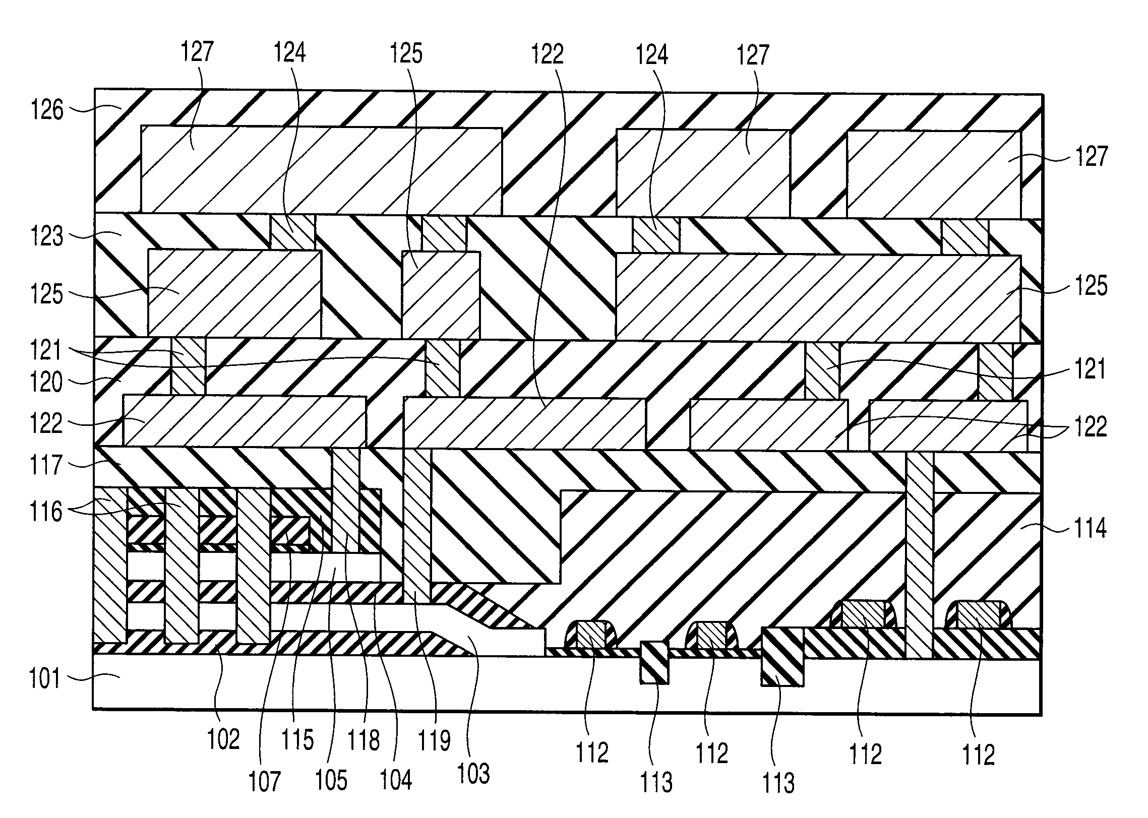
[0095]Each of FIGS. 1 to 7 is a perspective, sectional, or plan view showing a semiconductor memory (flash memory) according to the first embodiment of the present invention in a predetermined main manufacturing step.

[0096]This embodiment is directed to a two-layered memory in which single-crystal silicon layers serving as AA regions are formed by solid-phase epitaxial growth.

[0097]First, as shown in FIG. 1, a silicon thermal oxide film 102 serving as an interlayer dielectric (ILD) is formed to have a thickness of, e.g., about 50 nm on a semiconductor substrate 101. Then, the conventional lithography technique and etching technique are used to expose portions of the substrate as seeds of solid-phase growth. An amorphous silicon film about, e.g., 60 nm thick is formed on the entire surface of the substrate. Subsequently, annealing is performed to cause solid-phase epitaxial growth of the amorphous silicon film from the exposed portions of the substrate, thereby forming a single-cryst...

second embodiment

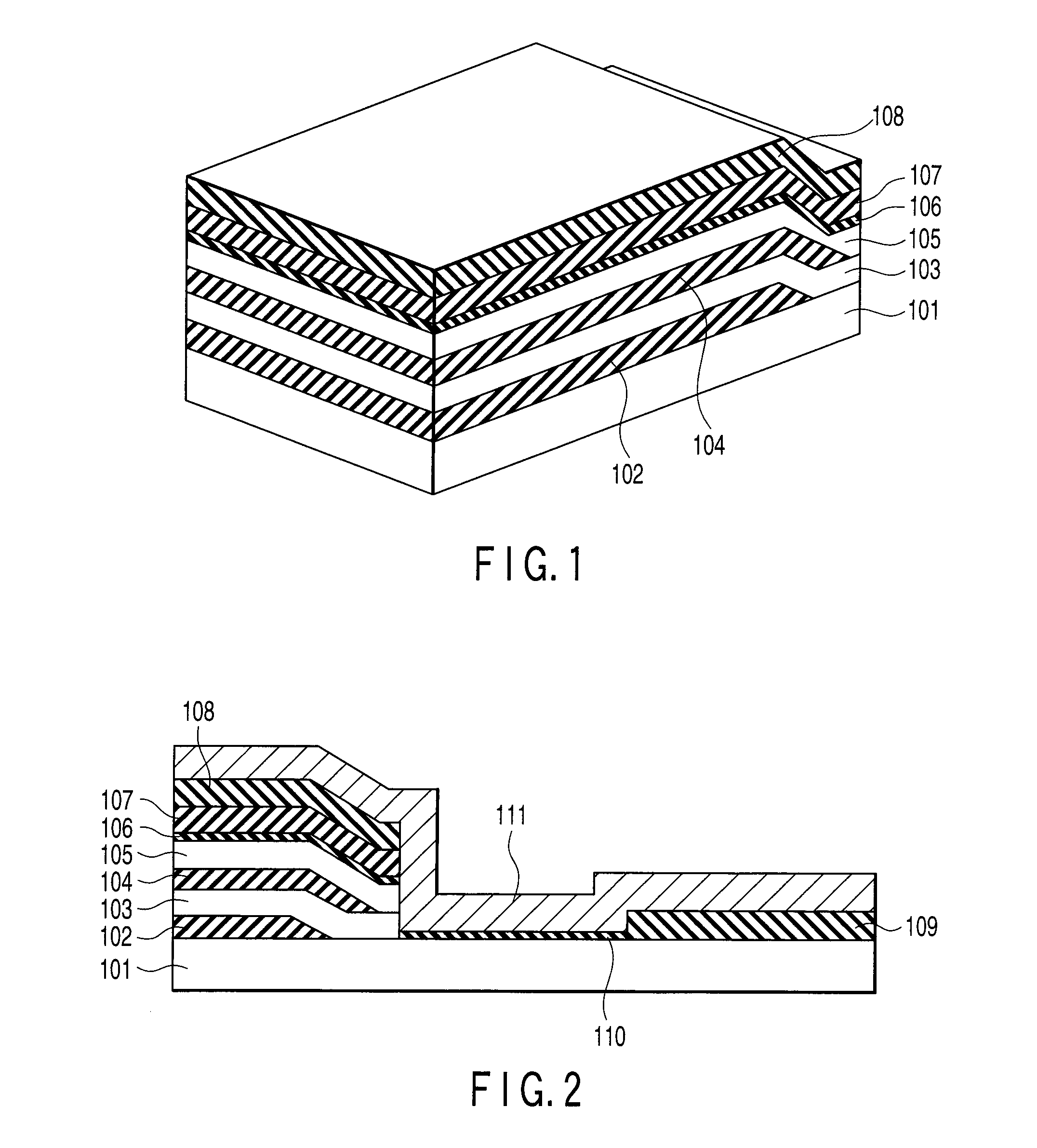
[0109]Each of FIGS. 8 to 13 is a perspective or sectional view showing a semiconductor memory (flash memory) according to the second embodiment of the present invention in a predetermined main manufacturing step.

[0110]This embodiment is directed to a four-layered memory in which single-crystal silicon layers serving as AA regions are formed by sequentially stacking and growing epitaxial silicon and epitaxial silicon germanium, and removing the silicon germanium films by selective etching.

[0111]First, as shown in FIG. 8, a first epitaxial silicon germanium film 202 about, e.g., 50 nm thick, first epitaxial silicon film 203 about, e.g., 60 nm thick, second epitaxial silicon germanium film 204 about, e.g., 50 nm thick, second epitaxial silicon film 205 about, e.g., 60 nm thick, third epitaxial silicon germanium film 206 about, e.g., 50 nm thick, third epitaxial silicon film 207 about, e.g., 60 nm thick, fourth epitaxial silicon germanium film 208 about, e.g., 50 nm thick, and fourth ep...

third embodiment

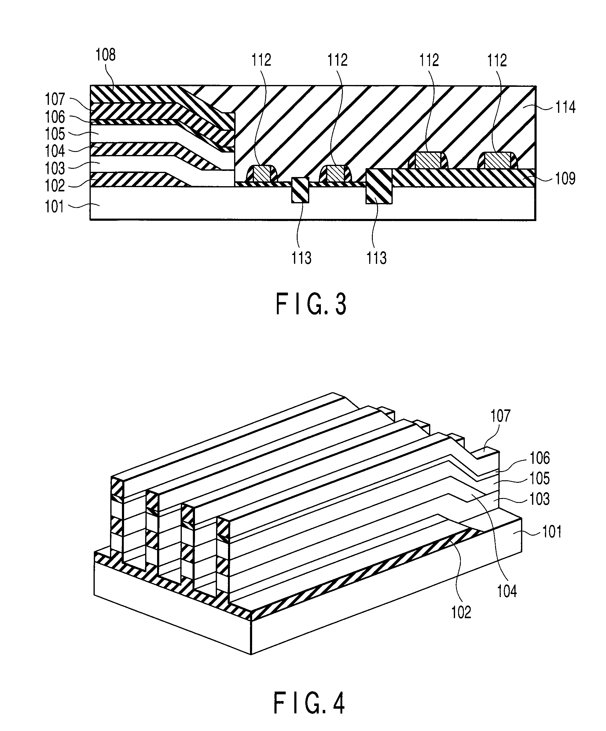
[0122]Each of FIGS. 14 to 19 is a perspective or sectional view showing a semiconductor memory (flash memory) according to the third embodiment of the present invention in a predetermined main manufacturing step.

[0123]This embodiment is directed to a four-layered memory similar to the second embodiment, but gate electrodes are processed by using the CMP technique.

[0124]First, as shown in FIG. 14, following the same procedure as in the second embodiment, four epitaxial silicon germanium films 302 and four epitaxial silicon films 303 are alternately stacked on a semiconductor substrate 301, and a silicon nitride film 304 and plasma CVD silicon oxide film 305 are formed on the layered epitaxial films. Then, the conventional lithography technique and etching technique are used to expose the end portions of the layered epitaxial films in a cell portion, and an epitaxial silicon film 306 is formed on the exposed portions. The silicon nitride film 304 and plasma CVD silicon oxide film 305 ...


PUM


Abstract

A semiconductor memory includes a plurality of stripe-like active areas formed by stacking, in a direction perpendicular to a substrate, a plurality of layers extending parallel to the substrate, a first gate electrode formed on first side surfaces of the active areas, the first side surfaces being perpendicular to the substrate, a second gate electrode formed on second side surfaces of the active areas, the second side surfaces being perpendicular to the substrate. The layers are patterned in self-alignment with each other, intersections of the active areas and the first gate electrode form a plurality of memory cells, and the plurality of memory cells in an intersecting plane share the first gate electrode.

Description

CROSS-REFERENCE TO RELATED APPLICATIONS[0001]This application is based upon and claims the benefit of priority from prior Japanese Patent Application No. 2006-256194, filed Sep. 21, 2006, the entire contents of which are incorporated herein by reference.BACKGROUND OF THE INVENTION[0002]1. Field of the Invention[0003]The present invention relates to a semiconductor memory and a method of manufacturing the same.[0004]2. Description of the Related Art[0005]Flash memories are widely used to store large-volume data in, e.g., cell phones, digital still cameras (DSCs), USB memories, and silicon audio, and the markets of these flash memories keep extending due to the reduction in manufacturing cost per bit (bit cost) resulting from rapid scaling of the device dimension. New applications are also rapidly rising. The result is a favorable cycle in which the rapid scaling-down and the reduction in manufacturing cost find new markets.[0006]In particular, a NAND flash memory has achieved a pract...

Claims


Application Information

Patent Timeline
Patent Type & Authority Applications(United States)
IPC IPC(8): H01L29/792H01L21/336
CPCH01L27/105H01L27/115H01L45/12H01L27/24H01L27/1052H01L27/11568H01L29/40117H10B63/845H10B63/20H10N70/823H10N70/231H10N70/20H10N70/8413H10N70/8828H10N70/8833H10N70/028H10B99/00H10B43/30H10B69/00H10B63/80H10B43/27H10B43/35H10B43/40H10B63/00H10B63/30H10N70/021H10N70/801H10N70/882H01L21/02532H01L21/02595H01L21/30604H01L21/31055H01L21/3212H01L21/32136H01L21/762H01L29/513H01L29/518
Inventor KIYOTOSHI, MASAHIROYAMAMOTO, AKIHITOOZAWA, YOSHIOARAI, FUMITAKASHIROTA, RIICHIRO
Owner KIOXIA CORP
Why Eureka
Try Eureka