Dielectric spacers for metal interconnects and method to form the same

a technology of dielectric spacers and metal interconnects, applied in the field of integrated circuits, can solve the problems of hammering affecting the structural integrity of a plurality of metal interconnects in the absence of supporting dielectric layers, and affecting the efficiency of metal interconnects

Active Publication Date: 2008-03-27
TAHOE RES LTD
View PDF37 Cites 46 Cited by
  • Summary
  • Abstract
  • Description
  • Claims
  • Application Information

AI Technical Summary

Problems solved by technology

Both of these factors hamper the efficiency of metal interconnects.
However, the incorporation of such films has proven to be challenging.
Although this technique has been effective for reducing the

Method used


Image

  • Dielectric spacers for metal interconnects and method to form the same
  • Dielectric spacers for metal interconnects and method to form the same
  • Dielectric spacers for metal interconnects and method to form the same

Examples


Embodiment Construction

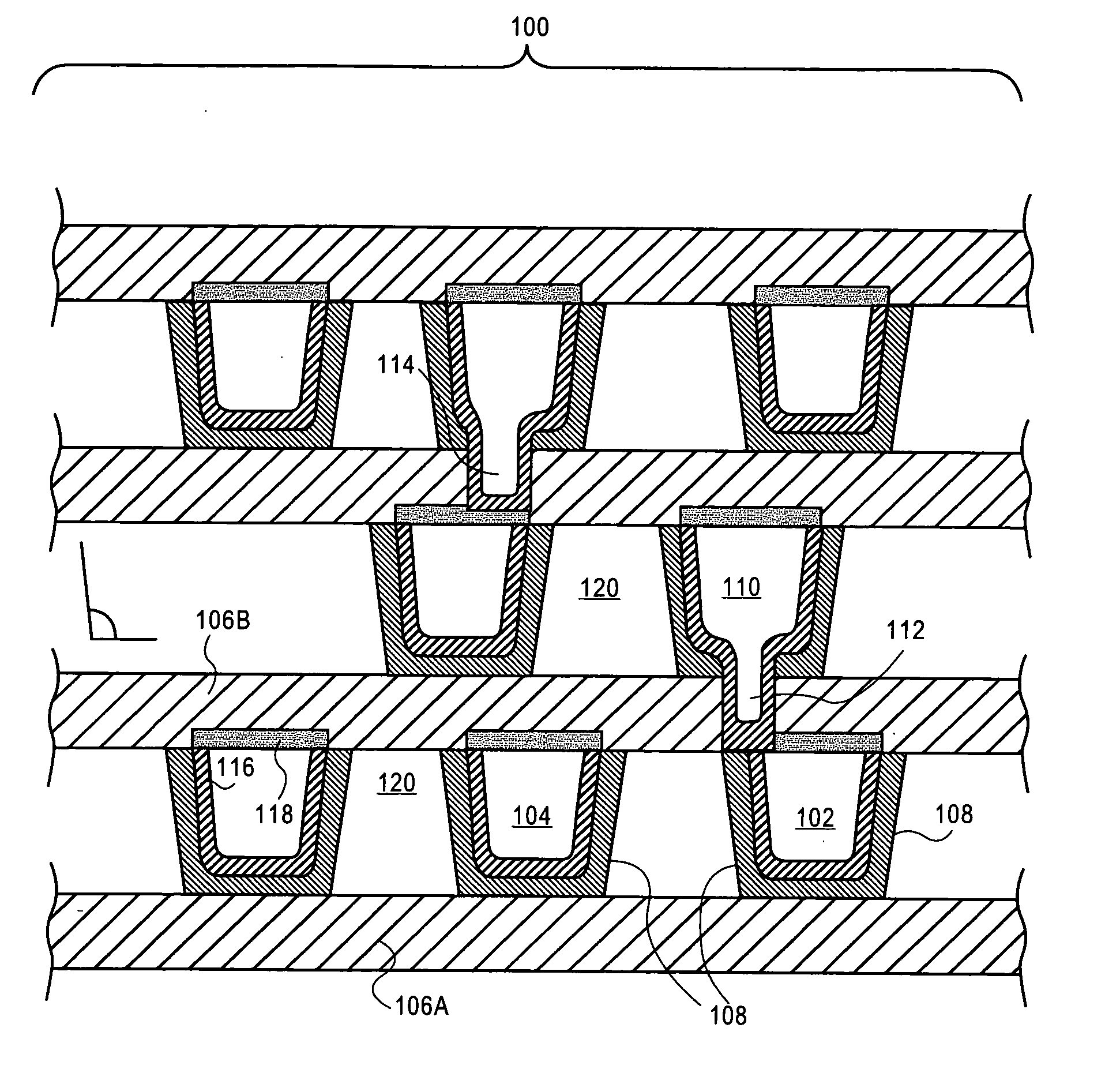
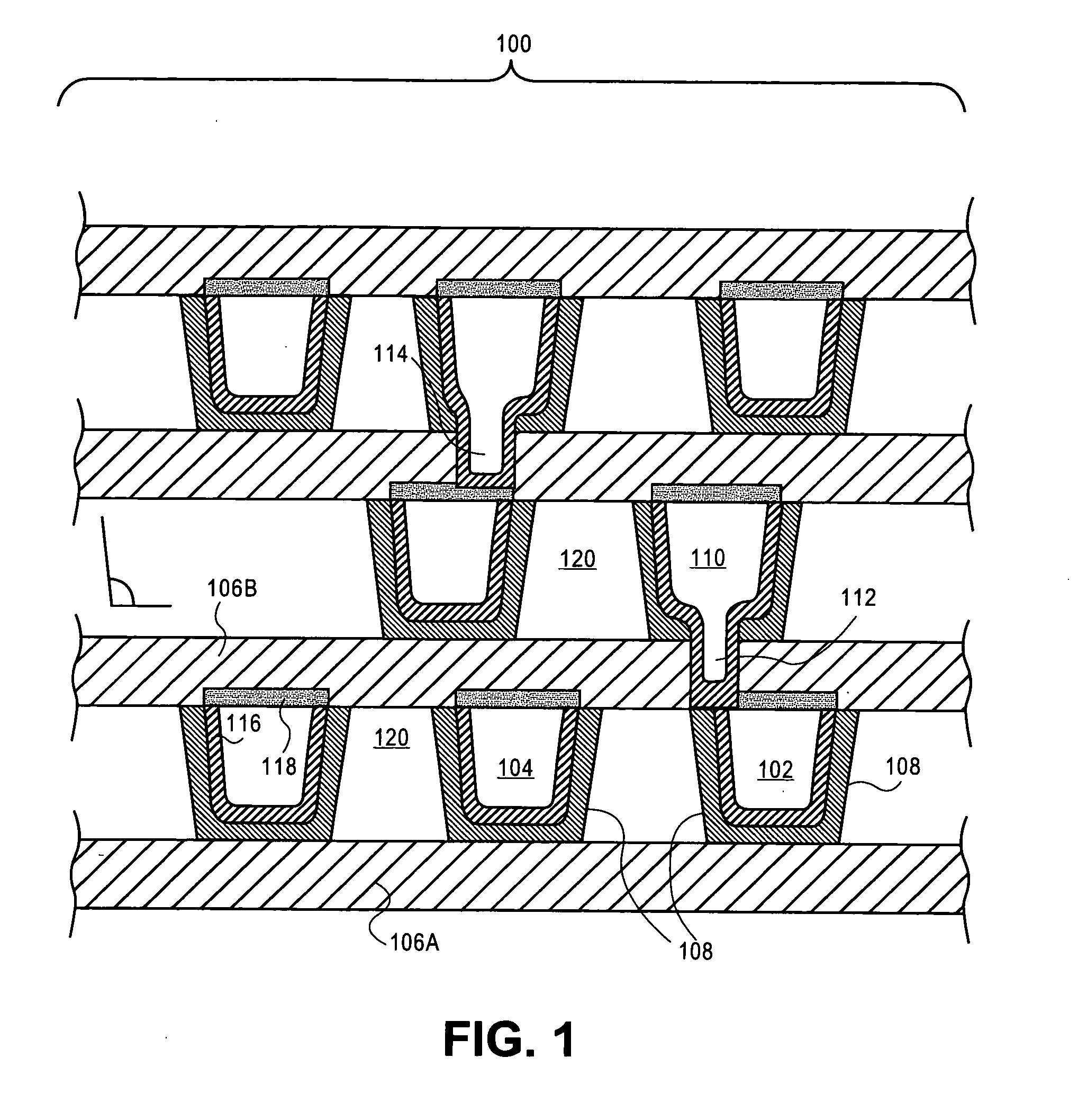
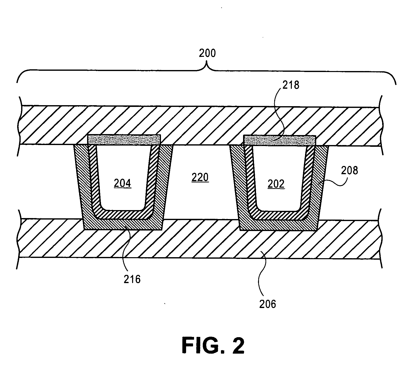
[0014]A plurality of metal interconnects with dielectric spacers for use in an integrated circuit and a process to fabricate such a plurality of metal interconnects are described. In the following description, numerous specific details are set forth, such as specific dimensions and chemical regimes, in order to provide a thorough understanding of the present invention. It will be apparent to one skilled in the art that the present invention may be practiced without these specific details. In other instances, well-known processing steps, such as patterning steps, are not described in detail, in order to not unnecessarily obscure the present invention. Furthermore, it is understood that the various embodiments shown in the figures are illustrative representations and are not necessarily drawn to scale.

[0015]Disclosed herein are dielectric spacers for metal interconnects and a method to form such dielectric spacers. Incorporating dielectric spacers adjacent to the sidewalls of metal in...


PUM


Abstract

Dielectric spacers for a plurality of metal interconnects and a method to form such dielectric spacers are described. In one embodiment, the dielectric spacers are adjacent to neighboring metal interconnects having flared profiles and are discontiguous from one another. In another embodiment, the dielectric spacers provide a region upon which un-landed vias may effectively land.

Description

BACKGROUND OF THE INVENTION[0001]1) Field of the Invention[0002]The invention is in the field of Integrated Circuits.[0003]2) Description of Related Art[0004]Metal interconnects are utilized in the fabrication of integrated circuits as a means of connecting various electronic and / or semiconductor devices into a global circuitry. Two key factors considered when fabricating such metal interconnects are the resistance (R) of each metal interconnect and the coupling capacitance (C), i.e. cross-talk, generated between the metal interconnects. Both of these factors hamper the efficiency of metal interconnects. Thus, it has been desirable to reduce both the resistance and the capacitance in metal interconnects in order to mitigate the so called “RC-delay.”[0005]For the past decade, the performance of integrated circuits, such as those found on microprocessors, has been greatly enhanced by the incorporation of copper interconnects into the “back-end” of line processing sequence. The presenc...

Claims


Application Information

Patent Timeline
IPC IPC(8): H01L29/00
CPCH01L21/76804H01L21/7682H01L21/76831H01L21/76885H01L23/5222H01L23/5283H01L2924/0002H01L23/53238H01L23/53276H01L23/53295H01L2924/00
Inventor BIELEFELD, JEFFERY D.BOYANOV, BOYAN
Owner TAHOE RES LTD
Why Eureka
Try Eureka