Low Mutual Inductance Matched Inductors

a mutual inductance and inductor technology, applied in the direction of low noise amplifiers, inductances, rf amplifiers, etc., to achieve the effect of reducing the overall chip geometry, reducing crosstalk, and improving component density

Active Publication Date: 2008-03-27
BELL SEMICON LLC
View PDF8 Cites 22 Cited by
  • Summary
  • Abstract
  • Description
  • Claims
  • Application Information

AI Technical Summary

Benefits of technology

[0014]Because the invention minimizes the crosstalk between inductors placed in close proximity to each other, the overall chip geometry may be reduced and component density improved. In implementations such as a DLNA, the counter wound inductor design having a common node may be utilized. These implementations help in maintaining the reliability of the circuit and components therein.

Problems solved by technology

In particular, the polarities of the magnetic fields produced by each inductor are opposite to each other so that at least a partial cancellation results when the fields interfere with each other.

Method used


Image

  • Low Mutual Inductance Matched Inductors
  • Low Mutual Inductance Matched Inductors
  • Low Mutual Inductance Matched Inductors

Examples


Embodiment Construction

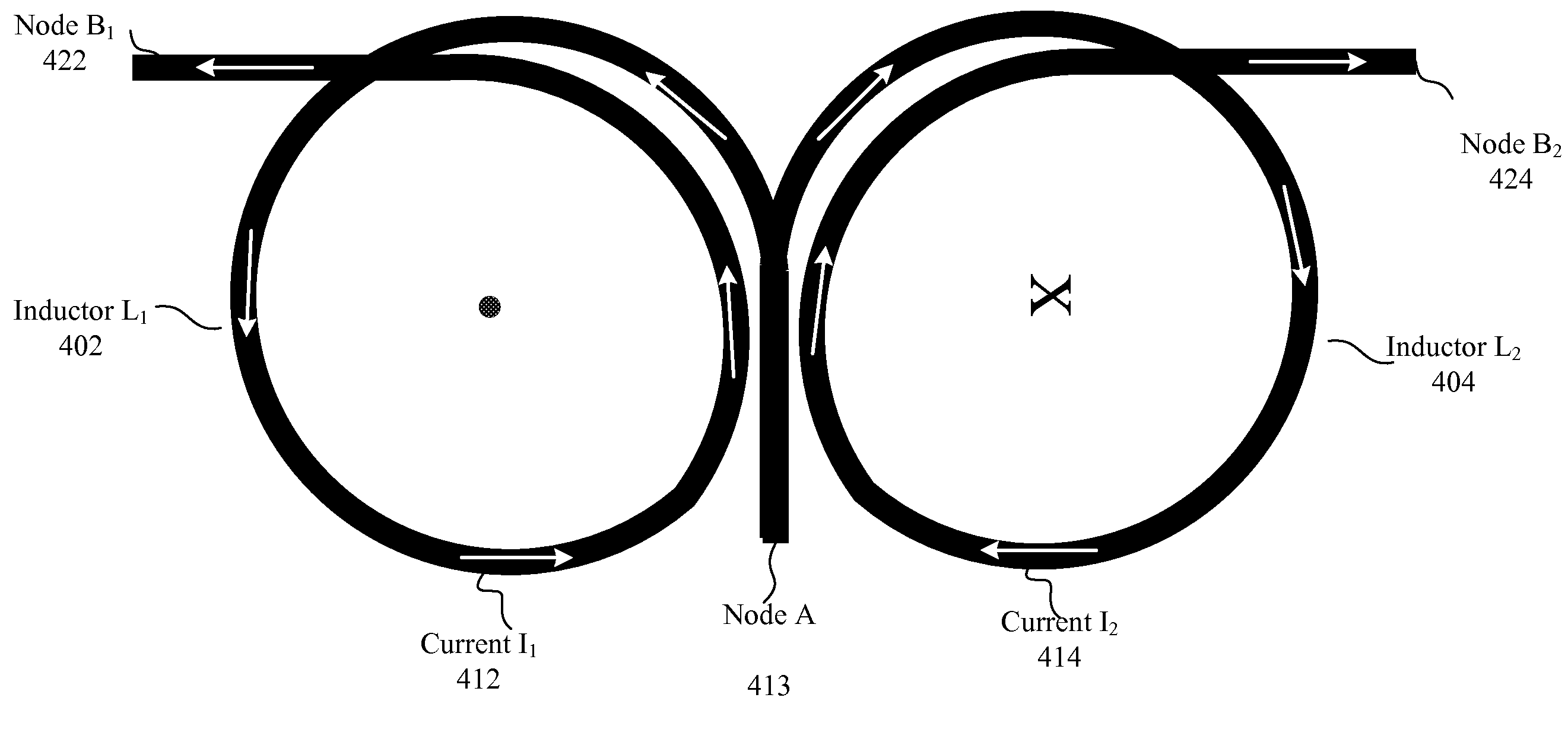
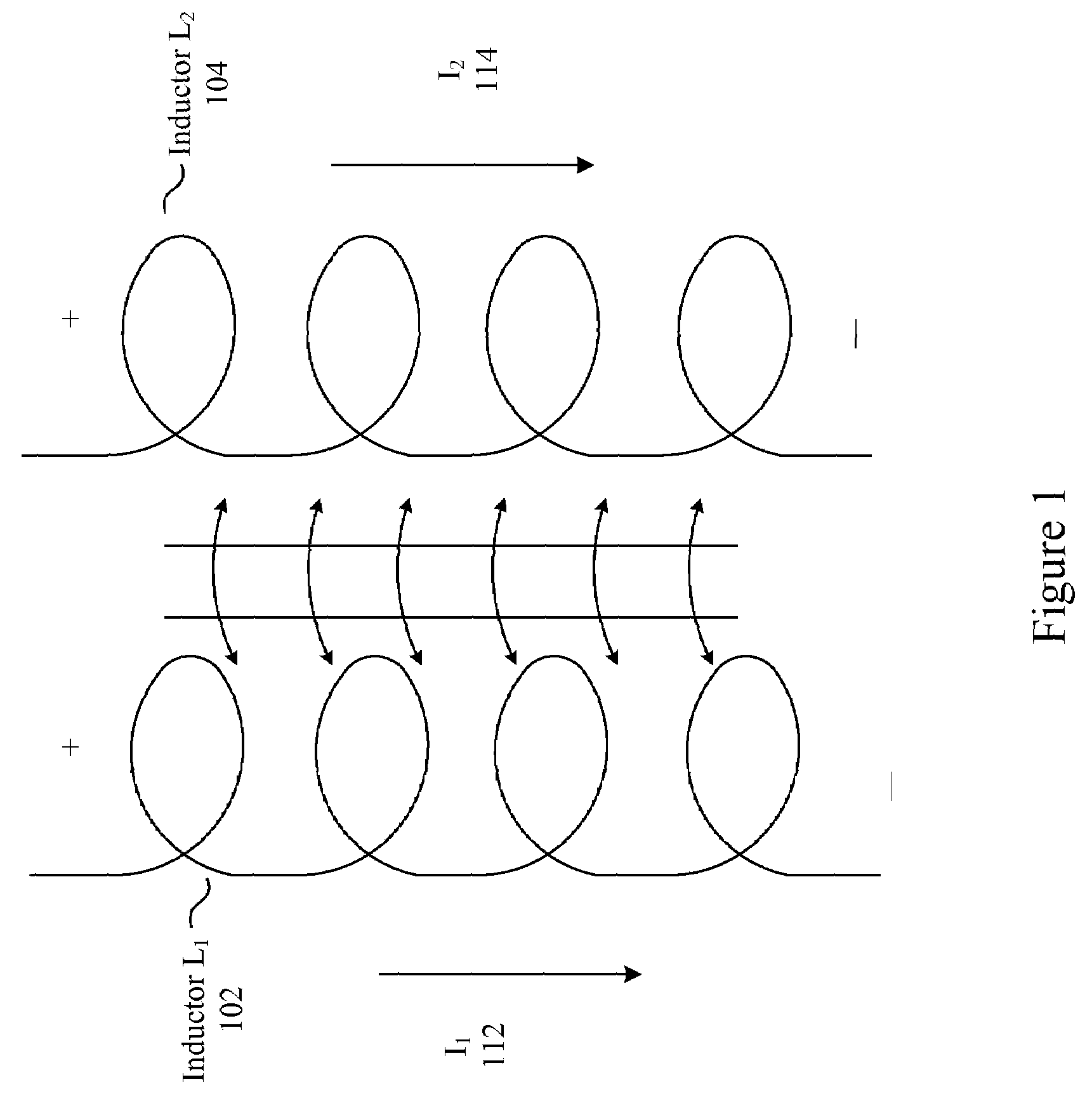
[0022]Multiple inductor structures and methods for providing low mutual inductance between the inductors are described. In various embodiments of the invention, the polarities of the inductors are positioned such that parasitic mutual inductance is reduced by causing electro-magnetic fields to at least partially cancel resulting in a reduction in interference between the inductors. The polarities of the magnetic fields produced by each inductor are opposite to each other so that at least a partial cancellation results when the fields interfere with each other. In certain embodiments of the invention, the inductors are counter wound and share a common node resulting in inverse polarities between the inductors. The inductors may be provided in various forms such as conventional octagonal, and conventional spiral.

[0023]In the following description, for purpose of explanation, specific details are set forth in order to provide an understanding of the invention. It will be apparent, howe...


PUM

PropertyMeasurementUnit
magnetic fieldaaaaaaaaaa
structuresaaaaaaaaaa
currentsaaaaaaaaaa

Abstract

Multiple inductor structures and methods for providing low mutual inductance between the inductors are described. In various embodiments of the invention, the polarities of the inductors are positioned such that parasitic mutual inductance is reduced by causing electro-magnetic fields to at least partially cancel resulting in a reduction in interference between the inductors. The polarities of the magnetic fields produced by each inductor are opposite to each other so that at least a partial cancellation results when the fields interfere with each other.

Description

BACKGROUND[0001]A. Technical Field[0002]This invention relates generally to electro-magnetic induction and interference, and more particularly, to the design of inductor coil elements within a semiconductor device.[0003]B. Background of the Invention[0004]Technological advancements in semiconductor manufacturing and electronic circuit design have resulted in a continual increase of component density within electrical circuits. These improvements in component density have resulted in a more efficient use of silicon area within the chip and a lower cost of production for each chip.[0005]As the proximity of electrical components increases, the affects of electrical cross-coupling or crosstalk may significantly degrade the performance of the circuit. The impact of electrical cross-coupling is a more significant issue in circuits that are operating at high frequencies. Oftentimes, these high speed circuits need to be specifically designed to address interference and cross-coupling in ord...

Claims


Application Information

Patent Timeline
Patent Type & Authority Applications(United States)
IPC IPC(8): H01F5/00
CPCH01F27/346H01F2017/0073H03F3/08H03F3/193H03F2203/45638H03F2200/294H03F2200/451H03F2203/45386H03F2203/45608H03F3/45188
Inventor ERICKSON, SEAN CHRISTOPHERHUDSON, JASON DEESAUNDERS, MICHAEL J.
Owner BELL SEMICON LLC
Why Eureka
Try Eureka